A Compact Meander-Bridge Electromagnetic Band-Gap Structure for Suppressing Simultaneous Switching Noise
Abstract
In this article, a new Meander-Bridge Electromagnetic Band-Gap Structure was proposed for the suppression of Simultaneously Switching Noises (SSN) over a wide frequency range, with dimensions of 15 x 15 mm and a useful area of 100 mm2. The equivalent model of the structure was created using lumped elements along with transmission lines. This method allowed determining the response characteristics across the entire frequency range of interest. Two boards were fabricated for conducting all the tests, including near-field and far-field measurements, S-parameter measurements, and electromagnetic wave simulations. The performance achieved a -30 dB level between the two ports in the frequency range of 1.75 to 11 GHz. To verify signal integrity, tests were conducted using ADS software at different communication rates, along with an internal near-field analysis of the PCB. Farfield measurements were also conducted experimentally. All the tests confirm the effectiveness of the proposed structure, demonstrating attenuation of SSN noise over a wide frequency band.
Index Terms
Eletromagnetic Band Gap (EBG); Power Integrity (PI); Signal Integrity (SI); Simultaneously Switching Noises (SSN).
I. INTRODUCTION
Nowadays most of the technological development, such as the Internet of Things (IoT), unmanned aerial vehicles (UAVs) and fifth-generation (5G) telecommunications networks, use high frequency electronics. These technologies require the use of multi-layer printed circuit boards (PCBs) that integrate digital and analog circuits. Furthermore, the integrated circuits comprising these boards must operate at frequencies above 1 GHz, providing high performance and increased functionality integration to handle the vast amount of data required by these applications [1].
During the switching of these digital circuits, there are high current transient spikes which occur primarily in CMOS integrated circuits with rise/fall edge rates in the range of tens of picoseconds and are commonly known as Simultaneously Switching Noises (SSN) [2] [3]. The power distribution network (PDN) is supposed to absorve these transients and keep the voltage supply stable, but due to imperfections of the PDN, spikes in the voltage can occur that can lead to malfunction of the circuits which share the same power bus [4]
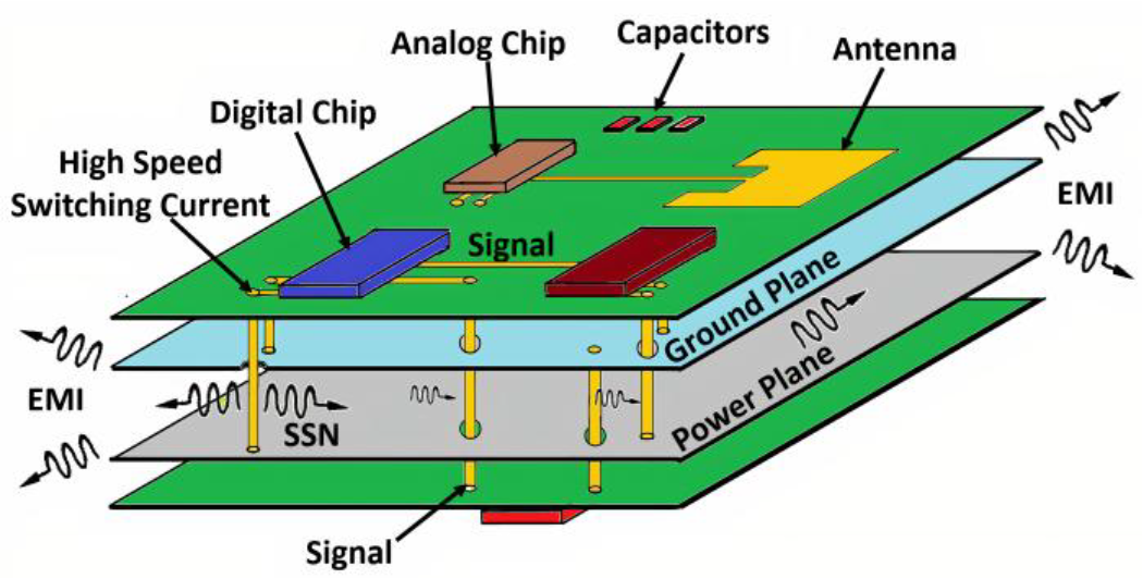
In addition to current and voltage spikes, the SSN noise generates electromagnetic radiation in the cavities formed by the power planes, where these planes act as waveguides, allowing the radiation to propagate throughout the entire board, as illustrated in Fig. 1 [5].

Consequently, SSN noise leads to Power Integrity (PI) and Signal Integrity (SI) issues in RF devices that are sensitive to noise, resulting in signal quality degradation, distortion, and data loss. Furthermore, as the electromagnetic radiation reaches the edges of the PCB, it is emitted into the surrounding environment. This causes electromagnetic interference onto other nearby electronic components as well as sensitive devices in the vicinity of the PCB [6] [5]. It is crucial to adopt efficient strategies for mitigating SSN noise over a wide operating bandwidth. These strategies are essential to minimize PI and SI problems, as well as to reduce the unwanted propagation of electromagnetic radiation on the PCB. [7] [8].
In recent decades, a wide range of studies have been conducted with the aim of mitigating the impact of electromagnetic radiation generated by SSN noise. Some traditional methods that provide significant suppression of electromagnetic waves at frequencies below 1 GHz include the use of decoupling capacitors [9], embedded capacitance [10], and split power planes [11].
To overcome the frequency limitation, the literature also explores the concept of developing PDN topologies with filtering behavior, such as the implementation of microstrip bandstop filters on the power and ground planes [12]. However, this option does not completely prevent the propagation of electromagnetic waves throughout the PCB’s entire extent.
Therefore, a more effective approach to suppress SSN that meets both aforementioned considerations is the use of the Electromagnetic Band Gap (EBG) structures [13]. These structures are periodically developed on the Power/Ground planes and have the ability to attenuate the propagation of electromagnetic waves in specific frequency bands [14]. A pioneering study in this area was presented by [15], where a compact and planar EBG was designed on the power plane, with an attenuation band from 0.8 to 4.9 GHz and an insertion loss below -20 dB.
The use of EBGs requires the insertion of multiple cells that are repeated along the axes, in order to achieve better performance in mitigating SSN over a wide operating frequency band [2] [16]. Thus, several studies have proposed modifications to the EBG structure in order to refine its suppression characteristics, such as the snake-shaped line EBG structure [17], Fractal EBG [18], T-bridge EBG [19], TSlit-EBG with CSRR [20], L-Bridge [7], Hybrid UC-EBG [21], and L-Bridge with NBCSRR [22]. These studies aim to broaden the suppression bandwidth and improve attenuation while maintaining a unit cell dimension of 30 x 30 mm. However, the continuous development of new electronic systems is characterized by PCB miniaturization [4], which poses a challenge for the application of EBG structures at such sizes.
Another option is the Double Square EBG [6], which has compact dimensions of 15 x 15 mm and a wide suppression frequency range. However, this result is only valid for the central rectangle of the structure, which is a 16 mm2 region. Therefore, if it is necessary to use this structure throughout the entire extent of the PCB, there may be a significant restriction on the available area for the design of electronic circuits.
In light of the above, it becomes necessary to explore new proposals for EBG structures that are smaller in size and maximize the available PCB area. This will allow for both localized use of the structure and its application throughout the entire board. The aim of this work is to design and implement a new structure called Meander-Bridge EBG (MB-EBG) with dimensions of 15x15 mm, a usable area of 100 mm2, and an attenuation band of 10 GHz with at least 30 dB of attenuation. The work is divided into the following sections: Section I presents the introduction, and in Section II, the development and analysis of the structure are demonstrated. Section III addresses the experimental results obtained, including attenuation measurements and the structure’s performance regarding signal integrity. Finally, in Section IV, the conclusion of the work is presented.
II. DEVELOPING AND ANALYSIS OF A MEANDER BRIDGE EBG DESIGN
A. Structure Design
The proposal is based on the traditional concept of an EBG structure that can provide SSN suppression capability. The newly developed structure has dimensions of 15x15 mm, and the specific details of a unit cell of the EBG are shown in Fig. 2.

The concept is to develop an Electromagnetic Band-Gap (EBG) structure where the central cell is maximized in size, while the connections have maximum length to increase the value of the equivalent inductance. The corresponding parameters are detailed in Table I.
B. Model of EBG
To evaluate the noise suppression properties of SSN in EBG structures, several methods have been proposed and widely discussed in the specialized literature. Among them, the following stand out: the cavity resonance model [23], which uses wave propagation principles in waveguides to determine resonant frequencies; the equivalent circuit model [24], which simplifies the EBG structure into lumped elements, facilitating analysis; the transmission line method combined with an equivalent circuit [25], which integrates propagation properties and the electrical response of the structure; and finally, the electromagnetic simulation method, widely used to predict the behavior of the structure under realistic conditions.
In this study, the method proposed by [25] was adopted to initially define the parameters and design of the structure due to the agility it provides in the development process. For simpler configurations, the method offers highly satisfactory results. In this specific case, the objective is to quickly determine the preliminary parameters of the structure, aiming to develop an EBG structure with an initial band below 3 GHz. This approach is particularly advantageous, considering that electromagnetic simulations can take several hours for each structural adjustment, whereas the lumped-element-based technique requires only a few seconds or minutes. Thus, the adopted method enables a faster and more efficient development of the initial parameters. Subsequently, an electromagnetic wave simulation was performed to validate the effectiveness of the proposed structure.
The equivalent circuit model of the EBG structure was implemented using lumped elements along with transmission lines of two adjacent cell units. These models were implemented in mathematical software using network analysis theories such as the Transmission (ABCD) matrix, Impedance Matrix, Admittance Matrix, and Scattering Matrix [26]. Fig. 3 illustrates the complete structure of two EBG cells connected in series.

Port 1 is positioned at the center of the patch and is connected to the four transmission lines. The characteristics of these transmission lines are modeled according to Equation 1.
Where d1 is the total size of the central patch and γ is the propagation constant, which takes into account the losses that occur when the signal passes through the dielectric [27]. This is represented by Equation 2.
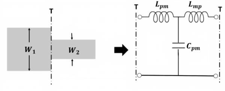
To determine the values of resistance (R), inductance (L), capacitance (C), and conductance (G), the equations provided by [28] are employed. Following that, there is the structure that represents the impedance transition between the patch and the meander, through the use of inductors (Lpm and Lmp) and a capacitor (Cpm), as illustrated in the Fig. 4.

The values of the inductors (Lpm and Lmp) and the capacitor (Cpm) can be determined by the following set of equations [26]:
The meander line is composed of N arms and N + 1 bridges connecting these arms, as illustrated in the Fig. 5. The width along the entire length of the meander is uniform and is designated as m4, while the distance between two adjacent arms is m2, and the length of each arm is m1. Additionally, the corresponding equivalent circuit model is presented, consisting of inductors (Lm) and capacitors (Cm and Cmi) [25].

The capacitor Cm is calculated as the sum of all capacitances between the stripline and the adjacent planes. The element Cmi represents the capacitance between the traces, the equations provided by [26] and [25] are employed. The inductor Lm is the sum of all the inductances present in the structure, such as self-inductance, mutual inductance, and image inductance. To account for the phase delay, a transmission line is included, where d2 is the length of the meander [25]. Finally, a resulting version is created with 24 sets of these blocks connected in series.
The next step involves defining the parameters Le1, Le2, and Cme of the structure that surrounds the entire central patch. This structure is formed by a set of connections between two traces that modify their thicknesses between two values. It is possible to model this element using the concept already presented of the discontinuity between two traces in conjunction with transmission lines to take into account the phase delay throughout the geometry. The size of this transmission line is defined by d3, which corresponds to the same dimension as s3.
After a series of tests aimed at reducing the initial frequency of the EBG filter to values below 3 GHz, the structure was implemented and simulated using the mathematical software (Octave). The simulation was performed in the frequency domain, covering the range from 1 MHz to 18 GHz with 1800 points, and completed in just 1.97 seconds. This performance is considered extremely efficient, enabling quick adjustments to the EBG structure parameters to achieve the most suitable response to the project specifications. Fig. 6 illustrates the insertion loss response (S21) of the modeled system, based on the parameters defined in Table I.

Simulation results of the S21 insertion loss for the proposed structure, obtained using the equivalent circuit model.
As analyzed in Fig. 6, the EBG structure demonstrated a consistent response within the frequencies of interest, particularly in the initial range from 1 MHz to 3 GHz, ensuring effective attenuation of SSN noise. One of the most significant advantages of the method used in this study is its ability to provide detailed information over a broader frequency range. In contrast, traditional approaches are typically limited to identifying the first resonance frequency, restricting the performance analysis of the structure across wider frequency bands.
III. SIMULATION, EXPERIMENTAL RESULTS, AND DISCUSSION
A. SSN Suppression Performance
To validate the effectiveness of the proposed structure, a four-layer PCB was designed. The two inner layers incorporate the EBG structure into their design and are dedicated to power distribution, while the two outer layers are intended for signal routing. The PCB configuration is illustrated in Fig. 7.

The proposed EBG structure was simulated and fabricated on a PCB with dimensions of 15 mm x 15 mm x 1 mm. The PCB material used is FR4, which has a dielectric constant of ɛr = 4.6 and a dissipation factor of tanδ = 0.02, as illustrated in Fig. 8a for the simulated model and in Fig. 8b for the fabricated board.

Top view of two adjacent EBG unit cells connected with an MB-bridge (a) simulated and (b) fabricated board.
In order to evaluate the effectiveness of the EBG structure in suppressing SSN, both experimental and simulation tests were conducted using two test ports positioned as shown in Fig. 8a and Fig. 8b. The performance of the proposed structure was simulated using the Advanced Design System (ADS) electromagnetic wave software, and experimental measurements were conducted using a Vector Network Analyzer (VNA) ENA E5063A to measure the transmission response (S21) of the EBG patterns. The measurement of insertion loss was performed, and the obtained results were compared with the simulation results, Fig. 9.

As seen in Fig. 9, the experimental EBG structure demonstrated a significant effect in suppressing the noise. It achieved an attenuation of approximately -30 dB in the frequency range from 1.75 GHz to 11 GHz.
The results overall show great similarity. In order to better compare and quantify how close the simulated response is to the experimental one, a test based on the IEEE Standard P1597.1. The S21 parameter was used to compare Feature Selective Validation (FSV), Amplitude Difference Measure (ADM) and Feature Difference Measure (FDM) [3], as shown in Fig. 9. For this comparison, the GRADE value is set to 5 and the SPREAD value is set to 4. These values represent the comparison between the levels of quality and reliability of the results.
As observed in Fig. 10a (ADM), approximately 35% of the data has equal amplitude, indicating agreement between the experimental and simulated results. Furthermore, nearly 70% of the data has a very close or equal amplitude difference to the expected value, which is considered very close or equal to the expected value.

FSV results for quantifying the difference between measured and simulated |S21| (a) Grade = 5 and spread = 4 for ADMc. (b) Grade = 5 and spread = 4 for FDMc
Regarding Fig. 10b (FDM), approximately 36% of the data show the same trend between experimental and simulated data. Additionally, around 61% of the data have a feature difference considered very close or equal, indicating a good match in the characteristics of the analyzed data.
The simulation using lumped elements is a technique that, for simpler EBG structures (with fewer branches), exhibits a response pattern very close to the real behavior, potentially coinciding entirely. In the context of this work, the obtained response was considered satisfactory across the entire analyzed frequency range, particularly in the initial frequency band, demonstrating good correspondence with experimental measurements. However, discrepancies were observed around 6 GHz and 17 GHz.
These differences can be attributed to the greater complexity of the analyzed structure and the number of branches present, which complicates precise modeling. In particular, the divergences may be explained by the absence of considerations regarding mutual inductance between more distant branches and the multiple capacitances existing between different branches of the structure. These interactions were not included in the model since the objective of this work was to use the method solely as an initial tool for determining the preliminary parameters of the EBG structure. Although these effects are more subtle, they become relevant at higher frequencies, impacting the accuracy of the simplified model.
Including these considerations in the model to achieve a more precise equivalence between methods exceeds the scope of this study, which focuses on using the method as an initial and efficient approach to defining the structure’s parameters.
Finally, the noise mitigation capability of the proposed structure is compared with some previous works, and the results are presented in Table II. The comparative analysis of the results demonstrates that the structure proposed in this study is capable of achieving similar or very close noise attenuations compared to the structures used in other studies. However, it is important to highlight that the significant advantage of the proposed structure lies in the fact that it occupies a much smaller area compared to the structures in previous studies. While most studies required an area of 900 mm2, the proposed structure in this study occupied only 225 mm2. Additionally, the distance between the analysis points is also significantly smaller, being up to nine times smaller in some cases compared to previous studies. These characteristics highlight the efficiency and space-saving aspect of the proposed structure, making it an attractive option for applications that require high noise attenuation with area and component spacing constraints.
B. SI Performance
The proposed EBG structure in this work achieves excellent SSN suppression results over a wide frequency range. However, the periodic slots in the EBG pattern will affect the continuity of the signal return path. As a result, signal transmission quality will degrade, leading to signal integrity issues.
In this section, the performance of signal integrity (SI) using the proposed EBG structure in this study is presented. To conduct this analysis, the ADS software is utilized, which applies a standardized signal of a 27-1 pseudo-random bit sequence (PRBS), non-return to zero, with a peak voltage of 0.5 V, a rise/fall time of 40 ps, and four different data transmission frequencies: 2.5 GHz, 5 GHz, 7.5 GHz, and 10 GHz.
The test signal is injected at Port 1, which is connected to a microstrip with a total length of 30 mm and a thickness of 0.37 mm, as shown in Fig. 11.
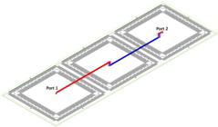
Four-layer structure with single-ended trace transit between the patterned power plane and the solid ground plane.
The path starts on the Top layer (red trace) and transitions to the Bottom layer (blue trace) using a via. The signal travels on the bottom layer and returns to the top layer through a second via, and the monitoring of the quality of the test signal transmission was performed at Port 2.
During the signal integrity evaluation, an eye diagram is generated, allowing for the determination of metrics such as the maximum eye open (MEO) and the maximum eye width (MEW). The MEO indicates the maximum eye opening and provides a measure of the amount of noise present in the signal. On the other hand, the MEW indicates the maximum eye width and is related to jitter. Typically, a larger MEO and MEW result in better signal integrity quality. Fig. 12 shows the responses of all analyzed structures and references.

Simulated eye patterns of the solid board and proposed MB-EBG board at different signal rates. Solid board: (a) 2.5 GHz, (c) 5.0 GHz, (e) 7.5 GHz, and (g) 10.0 GHz. The proposed board: (b) 2.5 GHz, (d) 5.0 GHz, (f) 7.5 GHz, and (h) 10.0 GHz
The corresponding SI metrics have been computed and are presented in Table III. In comparison with the reference, the worst case occurs at the frequency of 10 GHz, Fig. 12h, where there is a degradation of approximately 25% in the MEO metric and 68% in the MEW metric.
Degradation in high-frequency systems is often caused by discontinuities in the power plane, such as bends or length misalignments, which generate significant common-mode noise and consequently EMI problems [29], [30]. In EBG structures, the use of larger meanders can be an effective solution for SSN suppression, as these elements increase the power plane impedance, reducing the filter’s initial band frequency. Furthermore, the use of multiple EBG cells contributes to raising the filter’s upper frequency by providing a higher cavity resonance frequency.
However, increasing the size of the meanders presents challenges, such as compromising current return, which directly affects signal integrity. This occurs because higher impedance makes current return more difficult, potentially causing significant variations that degrade the structure’s electrical performance.
One solution to mitigate these issues is adopting differential communication, widely used in highspeed digital systems. Due to its balanced nature, differential communication is more tolerant to noise, such as crosstalk, interference from the power/ground plane, and noise generated by non-ideal return paths [29].
Another viable strategy is the use of EBG structures with shorter meanders, which reduce the negative impact on current return, or the implementation of a structure with constant impedance along its length, minimizing signal reflections. Structures with high impedance throughout their length hinder current return but can be optimized to balance noise suppression and signal integrity [31].
These approaches allow for combining noise suppression efficiency with the preservation of signal integrity, making them promising alternatives to overcome the limitations imposed by discontinuities and the increased size of meanders in EBG structures.
C. Internal Electric and Magnetic Fields of the PCB
With the help of ADS software, it was possible to perform a near-field analysis between the internal power layers of the PCB. For this purpose, two new PCBs were developed: a reference multilayer PCB with smooth power planes and another containing 9 cells of the EBG structure. Both used the same layer spacing as employed in the previous PCB, as shown in Fig. 13.
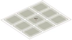
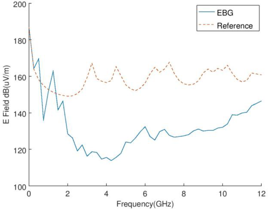
At Port 1 of the PCB, sinusoidal signals with a peak voltage of 1V were injected, covering the frequency range from 0.45 GHz to 18 GHz with a linear spacing of 0.45 GHz between them. Fig. 14 shows the graphs of the obtained results from the simulation of the electric fields in dB(uV/m). The values were calculated by averaging the values for each frequency in a region that corresponds to the 8 EBG structures around the central region. The orange line represents the reference, while the blue line represents the EBG structure.

As demonstrated, the reference board has an electric field ranging from 140 to 166 dB(uV/m) throughout the frequency range, while the PCB with EBG structure has values ranging from 118 to 140 dB(uV/m) in the range of 2 GHz to 10 GHz. Furthermore, it can be observed that the EBG structure, at certain frequencies such as 4 GHz, achieved an attenuation of approximately 40 dB compared to the reference. The performance of the EBG structure was superior across the entire proposed frequency range in this study when compared to the reference.
In Fig. 15, the results of the simulations for the magnetic field in dB(A/m) are shown in the frequency range from 0 to 18 GHz. As depicted in the first graph, the orange and blue lines represent the reference and EBG structure, respectively. The EBG PCB maintained magnetic field values below -30 dB(A/m) for almost the entire frequency range, with an average intensity of -35 dB(A/m). On the other hand, the reference PCB exhibited a distribution of field values with an average of -5 dB(A/m), remaining at approximately above -10 dB(A/m) in most of the analyzed points.

The results of the electromagnetic simulations for the frequency range of 0 to 18 GHz of the electric and magnetic near fields confirm that the use of the EBG structure attenuates the radiation originating from the SSN source over a wide frequency range. This prevents these electromagnetic fields from propagating through the internal layers of the PCB and interfering with sensitive electronic devices.
D. EMI Performance
In this section, the performance of the proposed EBG structure for attenuating the far-field around the PCB will be experimentally evaluated. The measurement setup for EMI in an anechoic chamber is illustrated in Fig. 16.

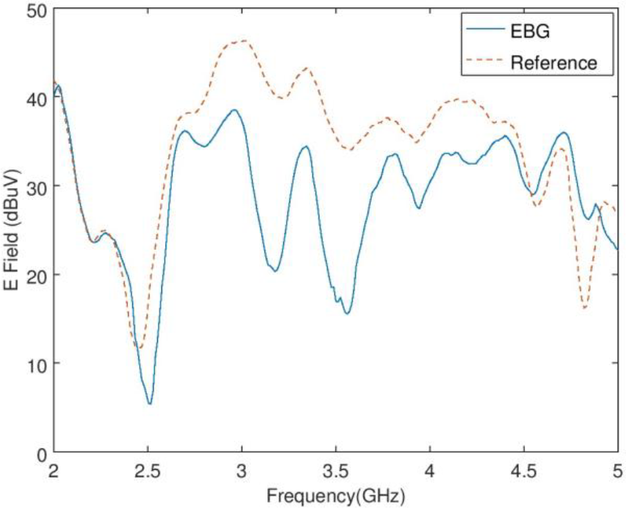
A horn antenna was used in this experiment, connected to the VNA ENA E5063A through calibrated coaxial cables and two 50-Ω ports. The same PCB model as in the previous section was positioned at a distance of 3 meters from the antenna. This setup allowed for the measurement of electromagnetic radiation as a function of the frequency, and the scatter parameter S21 was measured to obtain the results. Cable losses and antenna behaviour were taken into account to correct the data and obtain the electric field from the S21 measurement. The same measurements were performed on the reference PCB. The results of both PCBs are shown in Fig. 17.

Far field EMI experimental results measured in an anechoic chamber with a broadband antenna 3 m apart from the PCB.
Indeed, the results obtained are consistent with other studies, indicating that in the frequency range of 2 to 4.5 GHz, the radiation emitted by the PCB with the EBG structure is lower compared to the reference PCB. This demonstrates the effectiveness of the EBG structure in reducing electromagnetic radiation and confirms its potential for EMI suppression.
IV. CONCLUSION
In this article, a new type of miniaturized planar Electromagnetic Band Gap (EBG) structure with a dual-ring connected by a meander was presented. The proposed structure demonstrated an effective elimination of SSN noise, with a 30 dB attenuation in the frequency range from 1.7 GHz to 11 GHz
The S21 parameter results indicated that the proposed structure achieved satisfactory outcomes compared to other studies. Additionally, the proposed structure occupied only 25% of the area in relation to a standard EBG structure. It is worth noting that the central area of the structure was six times larger compared to another study with equivalent EBG dimensions, allowing for better space utilization on the PCB in future projects.
The signal integrity test was conducted at four different transmission rates: 2.5 GHz, 5 GHz, 7.5
GHz, and 10 GHz. In the best case scenario, at a frequency of 2.5 GHz, the proposed structure, Fig. 12b, exhibited a degradation of 8% in MEO and 45% in MEW compared to a reference board, Fig. 12a. These results indicate that the proposed structure maintains an acceptable signal transmission quality at different transmission rates.
The internal near-field test of the PCB showed that the EBG proposal resulted in 16% lower values for the electric field and nearly 7 times lower values for the magnetic field. Finally, a far-field test was performed, which demonstrated that the proposed structure reduced the electromagnetic radiation emitted at the edges of the PCB.
Indeed, the benefits of the proposed miniaturization of the EBG structure include its application in smaller PCBs, enabling a higher quantity of structures in series, and consequently, greater noise attenuation. Moreover, a smaller EBG allows for localized use of the structure, which improves signal integrity response in specific regions of the PCB
Overall, the results presented in this study demonstrate that the proposed EBG structure is effective in noise suppression over a wide frequency range and achieved satisfactory results in far-field radiation tests.
REFERENCES
- [1] P. Heydari, “Terahertz integrated circuits and systems for high-speed wireless communications: Challenges and design perspectives,” IEEE Open Journal of the Solid-State Circuits Society, vol. 1, pp. 18-36, 2021.
- [2] H.-R. Zhu, Y.-F. Sun, Z.-X. Huang, and X.-L. Wu, “A compact ebg structure with etching spiral slots for ultrawideband simultaneous switching noise mitigation in mixed signal systems,” IEEE Transactions on Components, Packaging and Manufacturing Technology, vol. 9, no. 8, pp. 1559-1567, 2019.
- [3] S. Jinno, S. Kitora, H. Toki, and M. Abe, “A mechanism of simultaneous switching noise in multiple plane conductors using two dimensional transport theory,” in Photonics Electromagnetics Research Symposium, pp. 2303-2307, 2019.
- [4] A. A. Y. Uma Maheswari and L. A. Kumar, “Noise mitigation in high-speed pcb applications: experimental verification and validation of electromagnetic band gap filters,” Journal of Electromagnetic Waves and Applications, vol. 36, no. 16, pp. 2320-2340, 2022.
- [5] S. Barth and A. K. Iyer, “A miniaturized uniplanar metamaterial-based ebg for parallel-plate mode suppression,” IEEE Transactions on Microwave Theory and Techniques, vol. 64, no. 4, pp. 1176-1185, 2016.
- [6] F. Zhang, P.-P. Ding, G.-M. Yang, and Y.-Q. Jin, “A novel double-square electromagnetic bandgap structure for wideband ssn suppression in high-speed pcb,” IEEE Transactions on Electromagnetic Compatibility, vol. 62, no. 6, pp. 2585-2594, 2020.
- [7] H.-R. Zhu, J.-B. Wang, Y.-F. Sun, X.-L. Wu, and J.-F. Mao, “A novel automatically designed ebg structure by improved ga for ultrawideband ssn mitigation of system in package,” IEEE Transactions on Components, Packaging and Manufacturing Technology, vol. 10, no. 1, pp. 123-133, 2020.
-
[8] P. Zuo, Y. Li, E.-P. Li, T. Song, M. Wang, and H. Zheng, “A novel electromagnetic bandgap design applied for suppression of printed circuit board electromagnetic radiation,” International Journal of RF and Microwave Computer-Aided Engineering, vol. 30, no. 1, p. n/a, 2020. [Online]. Available: https://onlinelibrary.wiley.com/doi/abs/10.1002/mmce.21990
» https://onlinelibrary.wiley.com/doi/abs/10.1002/mmce.21990 - [9] I. Erdin and R. Achar, “An effective global approach for assessment of decoupling capacitors on mixed planar and transmission line pdns,” IEEE Journal on Multiscale and Multiphysics Computational Techniques, vol. 7, pp. 176-185, 2022.
- [10] C. F. Yee, “The advantages of substituting decoupling capacitors on pwb with embedded capacitance technology,” in IEEE International RF and Microwave Conference, pp. 1-4, 2020.
- [11] Y.-E. Ho, H.-H. Hsu, J. Liao, and X. Cai, “Stitching impedance analysis of lpddr power plane split and its impact to radio frequency interference (rfi) and signal integrity (si),” in IEEE 26th Conference on Electrical Performance of Electronic Packaging and Systems, pp. 1-3, 2017.
- [12] S. Telikepalli, M. Swaminathan, and D. Keezer, “A simple technique for power distribution with better characteristics than electromagnetic bandgap structures,” IEEE Transactions on Components, Packaging and Manufacturing Technology, vol. 5, no. 6, pp. 797-805, 2015.
- [13] D.-B. Lin, H.-C. Lin, L.-Z. Zheng, and T.-H. Wang, “Segmentation method for modeling heterogeneous components to suppress broadband simultaneous switching noise on a multilayer structure,” IEEE Transactions on Components, Packaging and Manufacturing Technology, vol. 12, no. 5, pp. 798-807, 2022.
- [14] C.-K. Shen and T.-L. Wu, “Compact hybrid open stub ebg structure for power noise suppression in wlan band,” in IEEE International Symposium on Electromagnetic Compatibility, pp. 991-996, 2015.
- [15] R. Abhari and G. Eleftheriades, “Metallo-dielectric electromagnetic bandgap structures for suppression and isolation of the parallel-plate noise in high-speed circuits,” IEEE Transactions on Microwave Theory and Techniques, vol. 51, no. 6, pp. 1629-1639, 2003.
- [16] P. Chen, Q. Wu, and S. Shi, “Planar ebg structure for broadband suppression of simultaneous switching noise,” in IEEE International Conference on Electronic Information and Communication Technology, pp. 578-582, 2016.
- [17] F. Tong, S. Yang, Z. Zhao, and W. Wang, “Design of conformal snake-shaped line based dicyclic nested electromagnetic bandgap structure for ssn suppression,” in Asia-Pacific International Symposium on Electromagnetic Compatibility, pp. 798-800, 2022.
- [18] H.-R. Zhu, Y.-L. Zhao, and Z.-K. He, “Fractal localized ebg structure intelligently optimized by k-grnn and ga method for signal and power integrity,” IEEE Transactions on Microwave Theory and Techniques, vol. 71, no. 6, pp. 2333-2346, 2023.
- [19] M. R. Bansode, R. Dahatonde, and S. S. Rathod, “Simultaneous switching noise reduction in high speed circuits,” in International Conference on Communication information and Computing Technology, pp. 1-4, 2021.
- [20] Y. Zhao and H. Zhu, “A novel ebg power plane structure for ultrawideband suppression of ssn in high speed circuits,” in Cross Strait Radio Science Wireless Technology Conference, pp. 1-3, 2020.
- [21] J. Joo, H. Y. Choi, and E. Song, “Design and modeling of hybrid uniplanar electromagnetic bandgap power planes for wide-band noise suppression on printed circuit boards,” IEEE Access, vol. 8, pp. 31614-31621, 2020.
- [22] H. Zhu, J. Wang, Y. Sun, and X.-L. Wu, “An improved genetic algorithm for optimizing ebg structure with ultra-wideband ssn suppression performance of mixed signal systems,” IEEE Access, vol. 8, pp. 26129-26138, 2020.
- [23] L. Raimondo, F. De Paulis, and A. Orlandi, “A simple and efficient design procedure for planar electromagnetic bandgap structures on printed circuit boards,” IEEE Transactions on Electromagnetic Compatibility, vol. 53, no. 2, pp. 482-490, 2011.
- [24] L.-F. Shi and D.-L. Zhou, “Selectively embedded electromagnetic bandgap structure for suppression of simultaneous switching noise,” IEEE Transactions on Electromagnetic Compatibility, vol. 56, no. 6, pp. 1370-1376, 2014.
- [25] B. Mohajer-Iravani and O. M. Ramahi, “Wideband circuit model for planar ebg structures,” IEEE Transactions on Advanced Packaging, vol. 33, no. 1, pp. 169-179, 2010.
-
[26] M. J. L. Jia-Sheng Hong, Transmission Lines and Components John Wiley Sons, Ltd, 2001, ch. 4, pp. 77-107. [Online]. Available: https://onlinelibrary.wiley.com/doi/abs/10.1002/0471221619.ch4
» https://onlinelibrary.wiley.com/doi/abs/10.1002/0471221619.ch4 -
[27] C. R. Paul, Radiated Emissions and Susceptibility John Wiley Sons, Ltd, 2005, pp. 503-557. [Online]. Available: https://onlinelibrary.wiley.com/doi/abs/10.1002/0471758159.ch8
» https://onlinelibrary.wiley.com/doi/abs/10.1002/0471758159.ch8 -
[28] H. L. H. Stephen H. Hall, Nonideal Conductor Models John Wiley Sons, Ltd, 2009, ch. 5, pp. 201-248. [Online]. Available: https://onlinelibrary.wiley.com/doi/abs/10.1002/9780470423899.ch5
» https://onlinelibrary.wiley.com/doi/abs/10.1002/9780470423899.ch5 - [29] P. Zhou, T. Zhang, and Y. Shi, “Overview of common-mode noise suppression techniques: From reflection to absorption,” IEEE Microwave Magazine, vol. 24, no. 3, pp. 34-43, 2023.
- [30] C. Paul, “A comparison of the contributions of common-mode and differential-mode currents in radiated emissions,” IEEE Transactions on Electromagnetic Compatibility, vol. 31, no. 2, pp. 189-193, 1989.
-
[31] H. W. Ott, Electromagnetic Compatibility Engineering John Wiley Sons, Ltd, 2009. [Online]. Available: https://onlinelibrary.wiley.com/doi/abs/10.1002/9780470508510.ch10
» https://onlinelibrary.wiley.com/doi/abs/10.1002/9780470508510.ch10