A Case Study of a Didactic Platform Experiments using Off-the-Shelf Hardware
ABSTRACT
This paper explores the essential role of power electronics in modern electrical engineering and emphasizes the need for practical, hands-on learning experiences. By utilizing an easily-accessible, modular educational platform consisting of the DSP TI C2000 LAUNCHXL-F280049C and the BOOSTXL-3PHGANINV three-phase inverter module from Texas Instruments, students can bridge the gap between theoretical knowledge and practical application. Detailed descriptions of the hardware, along with case studies on a bidirectional boost converter and a three-phase inverter, illustrate the effectiveness of this approach. The findings show that integrating experiential learning methodologies significantly enhances student engagement and comprehension. The platform enables students to simulate, prototype, and experimentally verify their designs, promoting a deeper understanding of power electronics principles. The paper concludes by highlighting the potential for expanding this educational framework to include additional modules and applications, thereby preparing students more effectively for the evolving demands of the power electronics industry.
KEYWORDS
Power electronics; hands-on learning; educational platform; experiential learning
I. INTRODUCTION
Power electronic converters have played an indisputable role in the electric power system over the past few decades. These converters are present in various applications, ranging from variable-speed motor drives to battery charging schemes. They can provide reactive power control in electrical grids with an increasing penetration of renewable, power-electronics-based sources and address power quality issues such as harmonics and unbalance. Furthermore, power electronics is also present in High Voltage Direct Current (HVDC) systems for energy transmission and in renewable energy conversion systems [1].
In the dynamic and ever-evolving field of electrical engineering, power electronics stands out as an important technology that deals with converting and controlling electric power efficiently and effectively from the source to its destiny [2]. This discipline is relevant in a wide range of applications, from renewable energy sources and electric vehicles to power systems and consumer electronics. Power electronics, being a multifaceted area of study, as shown in in Fig. 1, consists of principles from electrical circuits, power systems, control systems and applied physics.

A wide range of methodologies, developed over the years by academia and industry experts, are reflected in the current educational scenario for learning power electronics. The gap in theoretical knowledge and its practical use has been increasingly recognized [3], [4], [5], [6] despite the robust fundamental understanding provided by classical education methods. As observed in [3], solely solving numerical problems related to common topologies used in power electronics is not sufficient, as this approach lacks the “hands-on” aspect of engineering. Additionally, as reported in [1], there has been a progressive lack of interest from new students in power engineering due to the lack of of experimental practice in laboratories. The discrepancy between practice and theory and the lack of motivation from students have led to a shift in educational practices focusing on experiential learning, with the aim of bridging this gap efficiently and making the learner the protagonist of their own learning [7].
In a field such as power electronics, the importance of matching theory and practice in learning can not be emphasized enough. It is widely known that a deep understanding of theoretical concepts and the ability to apply such concepts in real-world scenarios constitute the foundation of a proficient and versatile engineer. This educational philosophy is supported by the principles of constructivism and constructionism, which state that learners build knowledge and meaning from their experiences [8].
As cited in [9], project-based learning (PBL) is grounded in the belief that humans construct new knowledge over a base of what they already know and of what they have experienced, which they make available through active participation and interaction with others. The authors in [7] mention that the proposition of the project forces the students to do a series of learning activities while developing a project. A study conducted by [10] demonstrated the need of more real-life approach to the teaching of power electronics, i.e., the need to develop the ability of students to transfer theoretical knowledge into industrial practice.
The project-based approach poses many advantages and challenges. As reported in [3], there is a struggle in the beginning, as students are often used to the language of textbooks, and not so much to the language used at expert engineering levels. Students often need to review topics learned in past courses and they soon realize that there is a big gap in “knowing something in theory” and “having it done in practice”. On the other hand, this approach helps students understand the difference between textbook circuit diagrams, which are simplified for didactic purposes, and schematic diagrams used for real world implementations.
The findings in [4], [11], [12] show that the use of teaching methodologies based on a real-life project has enhanced students ability to interpret measurements correctly and compare them to simulation and theoretical results. It has also contributed to solidifying some concepts such as three-phase PWM generation, isolated drives and basic control. Additionally, the authors describe that the use of this approach helped motivate students and attract new ones to work on the field of power electronics. Students in [11] reported high levels of engagement and satisfaction, transforming theoretical knowledge into practical solutions for real-world problems. The methodological difference in the previously mentioned study was the focus on making a real-project, rather than the usual practice of simple repetition of predetermined experiments.
A review of how other institutions are using experimental setups to teach power electronics can be seen in [13]. The authors from this paper also proposed the design and implementation of full-bridge modules which can be used as different types of converters. The project of the dc-link voltage measurement, the isolated power supply and the bypass circuits have also been carried out. The reason for building this system is to make it possible to validate simulations and models using experimental setups. These setups highlight some physical characteristics of the systems, such as parasitic effects, which are challenging to replicate in Hardware-in-the-Loop (HIL) or simulations. These effects can significantly impact converter performance.
The authors in [1] proposed a detailed project to build and apply a modular educational kit to be used by research personnel and in the laboratory classes in power electronics with emphasis on medium voltage applications. This educational kit is based on the half-bridge topology, which is very flexible. The researchers also acknowledge that even though simulation is a risk-free environment for students, it is imperative for the learners to develop more feeling about the experiment. A similar approach has been seen in [5], where the author built a modular educational kit to teach dc-dc converters.
Computer simulations, widely used in the power electronics, are a powerful tool for circuit analysis as long as they have a strong correlation with experimental results [14]. Although computational tools are highly relevant, the construction of real-life prototypes cannot be underestimated since it serves a dual purpose [15]. Firstly, it connects theory and practice by providing applications of abstract concepts. Secondly, it contributes to higher quality research publications and validation, highlighting the importance of empirical evidence in the advancement of knowledge.
The work of [16] shows how the software PLECS and DSPs from Texas Instruments can be used to enhance the teaching and learning of power electronics and feedback control. By employing a teaching philosophy based on four pillars: (1) theory, (2) offline simulations, (3) hardware-in-the-loop testing, and (4) experimental verification, instructors were able to to emulate practices and design workflows that are already followed by industry. The authors built a robust and flexible platform to conduct experimental verification. As a result, it has been found that students are much more engaged when the problem they are working on can be associated with an application that they can understand, visualize, and relate to. The disadvantage of this framework is that the experimental verification platform may entail very high costs.
There is a lack of low-cost practical apparatuses to support the teaching of power electronics [6] and [17]. Addressing the challenges and opportunities within this educational context, this paper introduces a solution to this problem: the utilization of easy-to-program hardware and software platforms, such as those provided by Texas Instruments and Plexim, respectively, for testing the validity of the theory of power electronics. These platforms offer cost-effective means for students to engage in hands-on experimentation and prototyping.
The aim of this paper is to present an easy-to-program and robust platform capable of developing the expertise of students and researchers in the areas of control, power electronics and industrial electric drives. As case studies, three different projects were implemented: a boost converter, a three-phase inverter and the control of a permanent magnet synchronous motor. The experiments were conducted at LEACOPI [18]. This work also serves as a guide for those who intend to use these platforms in their laboratory tasks.
This paper is organized as follows: Section II provides a comprehensive description of the hardware used in the experimental platform, including details on the DSP TI C2000 LAUNCHXL-F280049C, the BOOSTXL-3PHGANINV Evaluation Module, and the PLECS software for simulation and modeling. Section III presents case studies, including the design and control of a bidirectional boost converter and a three-phase inverter, with detailed descriptions of the control structures and experimental setups. The results in Section IV analyze the performance of the experimental setups, showcasing the reference tracking, load disturbance rejection, and motor control tests. This section highlights the effectiveness of the proposed platform in bridging the gap between theoretical knowledge and practical application in power electronics. In Section V, a cost analysis was approached regarding the proposed didactic platform, as well as the authors view on the structure that should be made available in advance for this purpose. Section VI discusses the extent of application and relevance of the platform. In addition, it presents educational institutions that already use and study the electronic converter developed in this paper. Finally, Section VII concludes the paper with a summary of findings and potential future work in this area.
II. HARDWARE DESCRIPTION
An electronic converter is a device capable of converting the input electrical energy from one form to another at the output. This is done to produce the desired voltage/current for the operation of the electrical system where it is inserted. Converter topologies allow the circuit regime to be changed (from dc - direct current - to ac - alternating current - or the opposite) and the input variable to be amplified or reduced. Some topologies stand out, for example the inverters, rectifiers and boost and buck converters.
In this work, it will be proposed the construction of an electronic converter by combining the DSP TI C2000 LAUNCHXL-F280049C with the BOOSTXL-3PHGANINV three-phase inverter module. Since it is a simple and complete platform to implement, the relevance of applying it for educational and research purposes will be discussed.
A. The platform used
1) DSP TI C2000 LAUNCHXL-F280049C
The LAUNCHXL-F280049C is a development board from Texas Instruments for the C2000 series of real-time controllers and F28004x devices. It is a digital signal processor (DSP) widely used for prototyping and preliminary analysis of some applications in engineering [19].
The pin layout of this DSP can be seen in the Fig. 2. The highlighted areas correspond to the possibilities of coupling it with the three-phase inverter module.

2) BOOSTXL-3PHGANINV Evaluation Module
The BOOSTXL-3PHGANINV module is a 48 V and 10 A three-phase inverter. The typical values of switching frequency for this inverter are 40 kHz to 100 kHz, as reported in [20]. Such a device is predominantly applied in precision drives where precise control is required. This module uses Gallium Nitride (GaN) semiconductor devices, which results in a compact inverter with relatively low energy losses [21].
The connection between the devices is made by aligning the BOOSTXL module connectors with the DSP pins, as illustrated in Fig. 3. Furthermore, specific pins are designated for particular functions within the proposed setup, as detailed in Table 1. Notably, Connection I (present in Fig. 3.a) is achieved by connecting the BOOSTXL module to the J1-J4 pin groups of the DSP. Conversely, Connection II (shown in Fig. 3.b) is established using the J5-J8 pin groups.

(a) Connection I between LAUNCHXL-F280049C DSP and module BOOSTXL-3PHGANINV module. (b) Connection II between the two structures. (c) LAUNCHXL-F280049C DSP connected to two BOOSTXL modules, constituting two inverters.
From the analysis of Table 1 and visualization of Fig. 4, it is pertinent to explain and show the function of each signal described in them:
-
\(i_a\), \(i_b\) and \(i_c\): represent the currents of phases A, B, and C, respectively, at the converter output. By using ADCs (analog-to-digital converters), these phase currents can be read through three shunt resistors available on the BOOSTXL module.
-
\(v_a\), \(v_b\), and \(v_c\): constitute the voltages of phases A, B, and C, respectively, delivered at the converter output. These voltages can be measured using ADCs.
-
\(v_{dc}\): represents the dc-link voltage, which is the voltage supplied by the dc source to the converter. This voltage can be measured using ADCINA5 or ADCINA6.
-
\(delta_1\), \(delta_2\), \(delta_3\), \(delta_4\), \(delta_5\) and \(delta_6\): represent complementary signals for PWM A (\(delta_1\) and \(delta_2\)), B (\(delta_3\) and \(delta_4\)) and C (\(delta_5\) and \(delta_6\)). These complementary signals are used to perform the converter switching. From the PWM modules, pulse sequences are produced for phases A, B and C.
-
PWM enable: represents the signal capable of activating or deactivating the PWM generation units. Using the signal delivered to GPIO 39 for Connection I or to GPIO 33 for Connection II, it is possible to activate (logic level 0) or deactivate (logic level 1) the pulses produced by the PWM units.
-
PCB OT alert: represents an over-temperature alert. The BOOSTXL module has an internal temperature sensor (TMP302). Through the internal programming of the converter and the reading of this sensor, a signal is sent to pin 34/54 of connector J4/J8, if the temperature exceeds a safety limit.
Schematic representation of the inverter bridge connected to the dc source and the load. In addition, the signals received and sent by the DSP to the circuit are also presented.
An important fact about the topology studied is that the DSP pins have multiple functions. Therefore, the elements described in Table 1 correspond to pins that had their functions selected to constitute the electronic converter topology together with the BOOSTXL module. The full set of pin functions can be found in [19].
In addition to attaching a single BOOSTXL module to the DSP, it is also possible to attach two modules to a single DSP. This allows the use of two independent three-phase inverters simultaneously: one connected via Connection I and the other via Connection II. This configuration is illustrated in Fig. 3.c.
3) PLECS Simulation software
This software is a simulation and modeling platform for power electronic systems and electrical circuits. It is provided by Plexim and has several extensions, with PLECS Standlone and PLECS Coder being used in the didactic platform. These extensions constitute a single software and provide a simulation environment for modeling complex electrical circuits and sophisticated controls. Additionally, PLECS enables real-time interaction (through external mode) with the DSP via USB connection, allowing users to modify parameters and dynamically observe system behavior through its graphical interface [22].
Furthermore, it is important to mention that PLECS can be accessed at no cost through student licenses. To obtain them, the educational institution must have an agreement with Plexim that includes the desired software packages.
The use of PLECS to implement the platform proposed in this paper is due to some advantages of this software. Among them, it is possible to highlight the presence of a library of functions intended for TI C2000 devices and the conversion of the block programming language developed in the software to C code. This C algorithm is sent to the DSP through the USB connection.
B. Relevant aspects
1) USB isolation block
The headers JP1, JP2 and JP3 act as isolation between the DSP and the connected USB. By default, all three jumpers (connected to JP1, JP2 and JP3) are shorted and, therefore, the DSP power is provided by the USB connection. Complete isolation between the device and the USB is achieved by removing the three jumpers.
The header JP1 is responsible for separating GND from the DSP and the connected USB. Meanwhile, JP2 separates the 3.3 V and JP3 separates the 5 V. In situations where power isolation is desired, the DSP power must be supplied by an external source. Fig. 4 shows the two DSP power-up modes. In this figure, the inside of the dashed rectangle represents external power, whereas power via USB is represented by the connection to a personal computer (PC). Choosing between one powering option and the other will depend on the type and objective of the application.
In the case of the experimental platform used in this paper, all three jumpers were removed (as can be seen in Fig. 5), and power came from a dc source connected to the 48 V and GND inputs of the BOOSTXL module.

Distribution of important DSP headers and switches, as well as indication of which headers should have a jumper or not. Furthermore, the interfaces of the EQEP modules (J12 and J13) are highlighted.
2) Electrical isolation between pin groups J1-J4 and J5-J8
The header JP8 is responsible for isolating the 3.3 V and 5 V from the DSP pin groups J5 and J7 respectively. This isolation may be necessary if two BOOSTXL modules are connected, and both supply power to the DSP. In this scenario, if the two JP8 jumpers are removed, there will be no electrical contact between the Connection I and Connection II, allowing the implementation of two independent inverters. By default, the two connections of header JP8 are shorted by jumpers, as shown in Fig. 5.
3) 3.3 V to 5 V converter
The header JP9 is responsible for isolating the output of the LaunchPad step-up voltage regulator. This regulator is capable of increasing the voltage from 3.3 V to 5 V and making it available to the DSP power pins, if no other source is supplying 5 V. Therefore, to use the voltage regulator, the header JP3 must not have a jumper connected.
On the experimental platform, as the header JP3 is isolated, it is necessary to add a jumper to JP9 (as shown in Fig. 5) so that 5 V can be supplied to the DSP. This power supply will be important for the EQEP headers J12 and J13.
4) Encoder connectors
The headers J12 and J13 are used for connecting and receiving signals (A, B and I) from two independent linear or rotary encoders. These signals are sent to the DSP EQEP modules, where they are read and transmitted. J12 is connected to EQEP1 and J13 is connected to EQEP2. The detailed description of the encoders connection and routing is summarized in Table 2.
To route these signals to the EQEP modules, it is needed to set certain switches present on the DSP board. Fig. 5 presents a summary of the states of these switches for the use of each EQEP module. Firstly, to use EQEP1, it is necessary to toggle the left switch of S3 (key on the J5/J7 side) to 0 (that is, position it downwards). Furthermore, it is also needed to toggle S4 to 1 (that is, position it upwards). From there, the QEP signals are routed to J12. To use EQEP2, it is necessary to position the right switch of S3 (key on the J6/J8 side) to 0 (that is, switch it downwards). With this, the EQEP signals are routed to J13.
Both EQEPs can be used simultaneously, which makes it possible to operate two encoders at the same time. To do this, the states of switches S3 and S4 must satisfy both configurations.
5) 3.3 V supply for the LaunchPad
The header J5 of the BOOSTXL module is responsible for supplying 3.3 V to the inverter, through pin J1-1 (Connection I) or J5-41 (Connection II) of the DSP. When J5 is populated with a jumper, 3.3 V is supplied to the LaunchPad, and when it is not, this supply stops. This is shown in Fig. 6.

It is important to highlight that, when a jumper is inserted in J5, it must be ensured that the DSP is not powered by the USB connection. Therefore, it is necessary to remove the jumpers present in headers JP1, JP2 and JP3, when J5 is shorted. Alternatively, if USB power is desired, the jumper connected to header J5 must be removed. In the documentation, this header is referred to as J6, however J5 is the denomination present on the BOOSTXL board.
6) Voltage and current measurements
On the studied platform, it is possible to read the output voltages (\(v_a\), \(v_b\) and \(v_c\)) and currents (\(i_a\), \(i_b\) and \(i_c\)) of the converter, as well as the dc-link voltage (\(v_{dc}\)). As shown in Fig. 4, analog to digital converters (ADC) are used for this, specifically those described in Table 2. These ADCs are capable of measuring output voltages and currents and sending this information to the software used in programming, such as PLECS.
However, the readings obtained by these ADCs do not correspond to the real values, due to the gains and offsets associated with the conditioning circuits. Therefore, for the correct measurement of \(i_a\), \(i_b\) and \(i_c\), it is necessary to apply a gain and an offset as described in (1). \(i_r\) represents the real value of the current at the inverter output and \(i_m\) corresponds to the value measured by the ADC.
Furthermore, for \(v_a\), \(v_b\), \(v_c\) and \(v_{dc}\), it is necessary to use a gain and an offset as shown in (2). \(v_r\) represents the real value and \(v_m\) corresponds to the value measured by the ADC.
Both \(i_m\) and \(v_m\) are within the interval of 0 V to 3 V, since this is the operating range of the ADC. The offsets and gains values were obtained experimentally, externally measuring the desired voltages and currents, and comparing them with the ADC readings. The values are similar to those obtained through conditioning circuit analysis following the information provided in [23].
7) Digital to analog converters
DACs A and B are digital-to-analog converters capable of synthesizing the signals delivered to them on specific DSP pins. In the LAUNCHXL-F280049C, there are two DACs. DAC A is located on pin J7-70 and DAC B on pin J3-30. Through programming, it is possible to send signals to the DACs, which will be made available externally in the range of 0 V to 3 V.
The use of DACs is the opposite of the connection to the BOOSTXL module. Therefore, if you are using Connection I, you must use DAC A, which is on pin J7-70 of Connection II. Similarly, if you are using Connection II, you must apply DAC B, which is on pin J3-30 of Connection I. This occurs because the DAC pin shares other functions, depending on the type of connection used. As a limitation of this platform, it can be mentioned that if two BOOSTXL are connected to the DSP, it is not possible to use the DACs, precisely because of the sharing of functions. The summary of DAC usage information is shown in Table 3.
III. CASE STUDIES
The association of the DSP with the BOOSTXL module is capable of implementing, in the same hardware, several electronic converter topologies depending on the code developed. This represents an advantage of the platform, in addition to stimulating its educational purpose, since in the same environment it is possible to teach different electronic converter configurations.
Considering the desired impact of this work, the authors considered the topologies of boost converter and three-phase inverter relevant and developed case studies for them. It is worth mentioning that the association of DSP with BOOSTXL module is not limited to these configurations. It is also possible to implement buck converters and single-phase and cascaded inverters, for example.
Through the exploration of the topologies chosen in this work, students will gain valuable insights into various fundamental concepts in power electronics. For instance, by working ac and dc converters, students will learn about control and modulation techniques. Additionally, students will acquire hands-on experience by implementing modulation techniques and control strategies to operate an electrical drive, thereby bridging the gap between theoretical knowledge and practical application.
A. Controlled bidirectional boost converter
Using the previously mentioned DSP in association with the BOOSTXL module, it is also possible to build a dc-dc converter by using one of the three arms of the BOOSTXL module. The control, as well as the measurements, are then carried out in the DSP.
A boost converter is a type of dc-dc converter used to step up the voltage level from a lower input voltage. It operates by storing energy in an inductor and then releasing it to the output as the switches commute. They can be used in battery-powered systems where a higher voltage is required than the one the battery can provide [2]. Fig. 7 presents a topology used to implement a bidirectional boost converter.

Topology of a bidirectional boost converter. The black lines represent power conductors and the green lines are measurement and control signals.
This topology has the following main components:
-
Controlled switches (\(S_1\) and \(S_2\)): the \(S_1\) and \(S_2\) switches are responsible for controlling the converter’s power flow. They always operate in a complementary manner, i.e. synchronous operation. They can be realized in practice by means of an IGBT (insulated-gate bipolar transistor) or a MOSFET (metal-oxide-semiconductor field-effect transistor). It should be noted that for the voltage level investigated (12 V battery), it is more common to use a MOSFET.
-
Inductor (\(L\)): the inductor is responsible for storing energy during the converter operation. It provides a smooth direct current. It should be noted that in the implementation investigated, the inductor current is the battery current itself.
-
Capacitor (\(C\)): the capacitor limits the ripple in the converter output voltage.
The control of the boost converter has the function of keeping the output voltage (\(v_o\)) constant around a reference value (\(v_o^*\)). A classic current mode control was used, where the internal (faster) loop regulates the converter inductor current, whereas the external (slower) loop controls the output voltage. Fig. 8 shows a diagram of these two loops.

For the current loop, the bandwidth was chosen as:
where \(f_{sw}\) is the switching frequency of the converter. Choosing 1/20 of the switching frequency reduces the effect of the implementation delay on the current loop response (in the order of 1 sampling period). Assuming a proportional integral controller and using pole placement technique, the following tuning equations can be derived:
where \(L\) is the value of the inductance of the converter, \(r_L\) is the value of the resistance of the inductor and \(v_{o,n}\) is the nominal output voltage of the converter.
For the voltage loop, the bandwidth \(f_v\) is defined by the equation:
Thus, assuming a proportional integral controller and using the pole placement technique, the gain for the voltage loop can be calculated by:
where \(C\) is the value of the capacitor, \(d_{avg}\) is the duty-cycle value and \(\overline{R}\) is a resistance that consumes nominal power from the converter given by:
where \(P_n\) is the nominal power of the converter.
B. Three-phase inverter
Three-phase inverters are dc-ac converters widely used in industrial applications, in drive control and power generation, for example. Properly activating this equipment is essential for the efficiency, stability and operation of the systems where it is included. In view of the growing application of inverters, this work will discuss the experimentation of a three-phase inverter from the DSP LAUNCHXL-F280049C and the BOOSTXL-3PHGANINV module, which will be applied in tests with a synchronous motor and an RL load.
The basic topology of this inverter consists of six semiconductor switches with six diodes in antiparallel, forming three arms as shown in Fig. 4. Each arm contains two semiconductor devices that receive complementary signals responsible for the inverter switching. By switching them in a specific order, it is possible to synthesize a desired waveform at the inverter output.
In this paper, the sinusoidal PWM modulation (SPWM) technique will be discussed. In this modulation technique, a reference sine wave is compared with a high-frequency triangular carrier. The result of this comparison is a variable pulse sequence (PWM) to be sent to the semiconductor switches. In the given application, three reference sine waves were used, \(2\pi/3\) rad out of phase with each other. From the comparison with the triangular waveform, three PWM signals were generated and sent to each of the inverter arms. In this modulation strategy, the reference sine wave is responsible for the fundamental frequency at the output, whereas the triangular carrier defines the switching frequency.
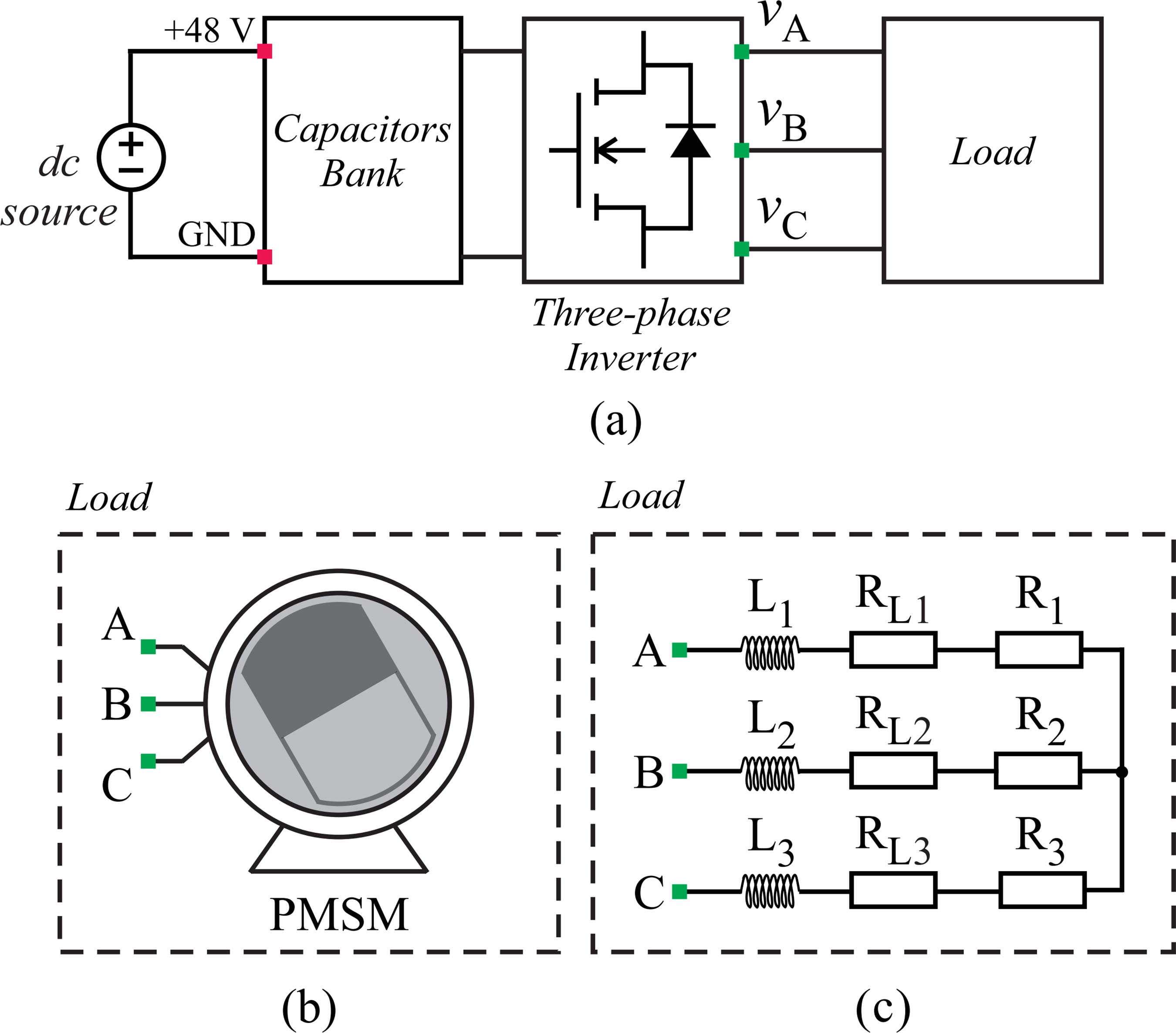
The overview of the setup assembled for the following tests can be seen in Fig. 9.a. One of the cases studied in this paper was the operation of the three-phase inverter with a Teknic M-2310P-LN-04K permanent magnet synchronous motor (PMSM). The connection diagram can be seen in Fig. 9.b. A notable point of this motor is the presence, internally, of an incremental encoder of 4000 counts/revolution. The connection between the encoder and the DSP is made by connecting the terminal J4 of the motor to the headers J12 or J13. The terminal J4 has the power supply (5 V and GND) and signal (A, B and I) wiring of the encoder. The mechanical speed and angle signals are obtained using a counter algorithm that counts the pulses emitted by the encoder. From these pulses, the counter synthesizes the angular position signal, which is sent to a derivative algorithm. By deriving it, the mechanical speed signal is produced.

(a) Schematic representation of the inverter connected to the dc source, the capacitor bank and the load. There are two loads, the first (b) represents the tests where the inverter is connected to the permanent magnet synchronous motor (PMSM), and the second (c) the tests with the star-connected RL load.
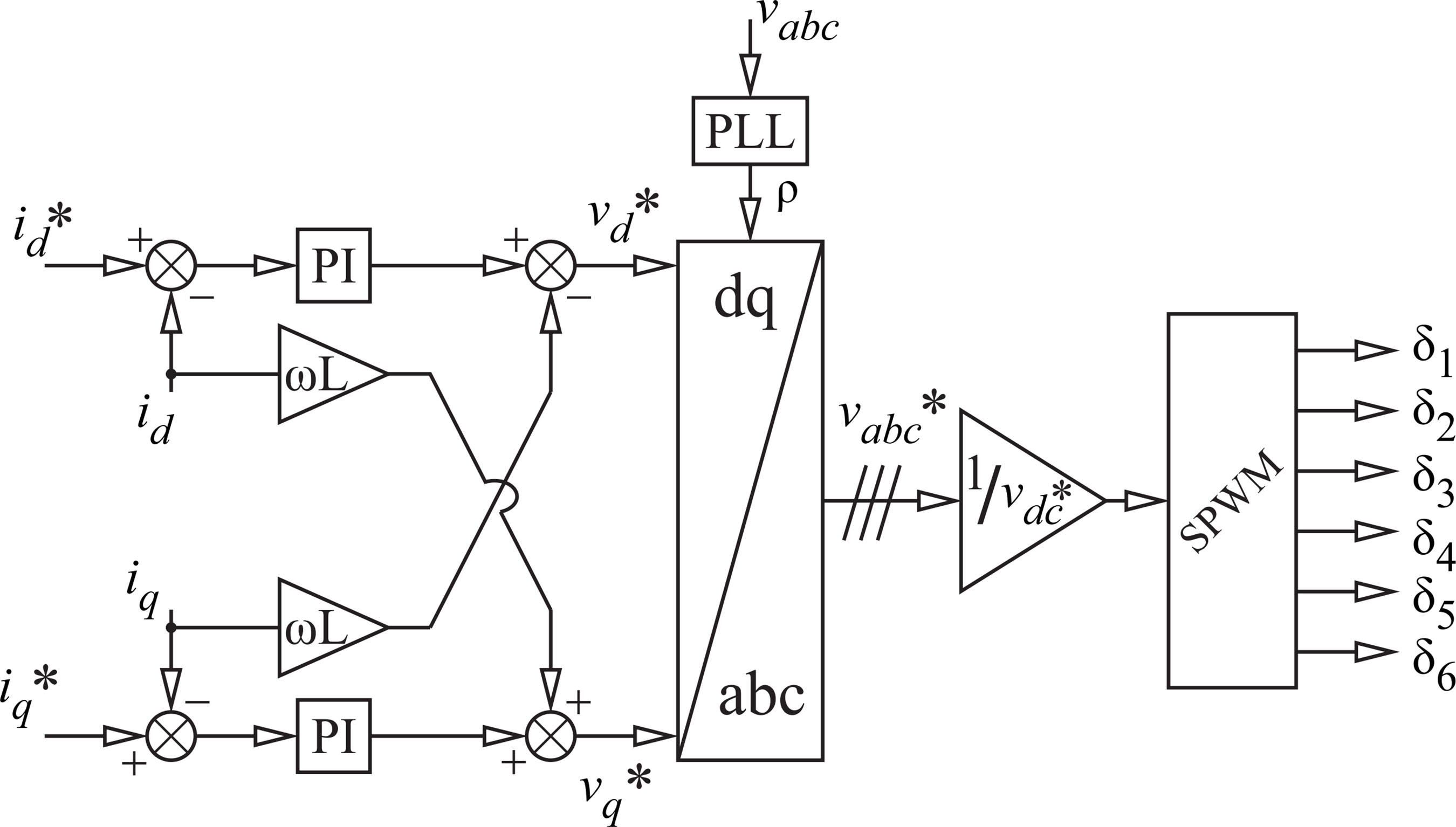
Furthermore, another case discussed was the development of a closed-loop current control. For this, the inverter was attached to a star-connected RL load. This setup is shown in Fig. 9.c. The control structure used in tests with the RL load can be seen in the Fig. 10. A current control in synchronous coordinates (dq) based on PI controllers was used. The phase-locked loop (PLL) is necessary in the control structure to synchronize the inverter with the grid. In short, this system determines the voltage that must be synthesized by the inverter, through the definition of the direct and quadrature axis currents. Based on this information and applying a modulation algorithm, the inverter switching is defined by signals \(\delta_1\)-\(\delta_6\).

The control tuning employes pole placement technique. The proportional and integral gains are given by:
where \(f_c\) is the b0ontroller.
IV. RESULTS
This section contains the results of the platform operating as a boost converter and a three-phase inverter. For each setup, the tests adopted different paths, reinforcing the relevance of the platform. To acquire these results, the oscilloscopes Tektronix TDS 1001C-EDU and RIGOL MSO5204 were used, as well as their respective voltage probes. Furthermore, current probes from a power quality analyzer model Fluke i-400s were applied to read the inverter output currents.
A. Controlled bidirectional boost converter
The parameters of the converter used in the simulation are shown in Table 4. The inductor parameters adopted refer to components available in the laboratory for building the prototype. The capacitance, on the other hand, is that already present in the BOOSTXL.
Using the parameters in Table 4 and Equations (3)-(8), the parameters of the controllers for both the current and voltage loops of the local control can be obtained, as shown in Table 5. The sampling is synchronized with the PWM carrier to obtain the average values of current and voltage. In this way, the signals are sampled at the moment they cross their average value. By using this technique, it is possible to eliminate the need for filters to estimate the average value of the measured quantities. The current limit of the battery was determined using the maximum current of the inductor, \(I_L\), informed by the manufacturer.
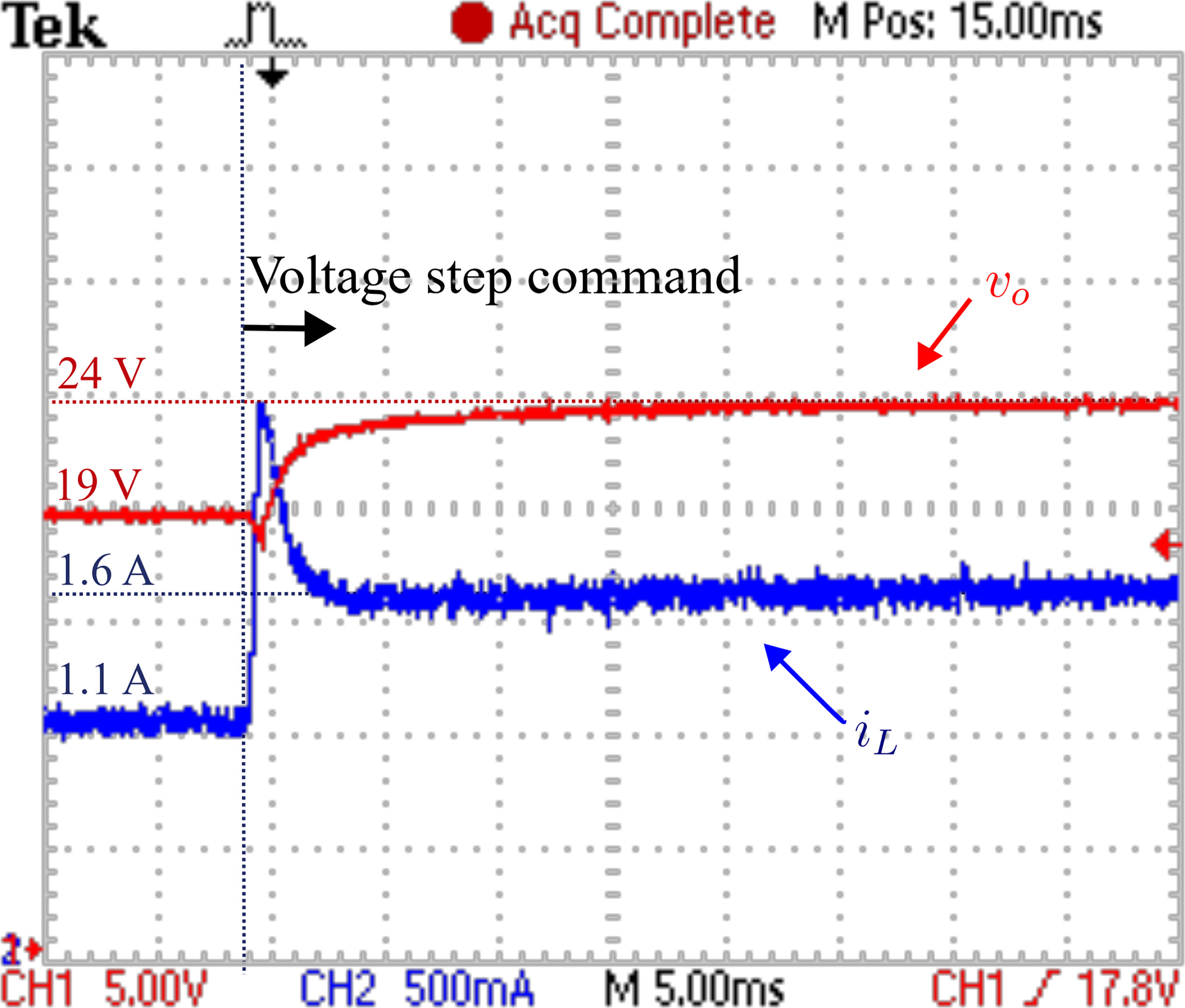
Using the component values specified in Table 4, the boost converter in Fig. 7 was implemented. The results for the reference following are shown in Fig. 11. Using the gains for the controllers obtained in Table 5, the boost converter was commanded to increase its output voltage from \(19~ ext{V}\) to \(24~ ext{V}\) near \(9~ ext{ms}\). In this setup, the load at the output was a \(16~\Omega\) resistor. It can be seen that the current, after a peak close to \(2.5~ ext{A}\), increased from \(1.1~ ext{A}\) to \(1.6~ ext{A}\). The phenomenon of non-minimum phase could also be observed in the voltage response, leading to a 10% decrease on the output voltage, \(v_o\).
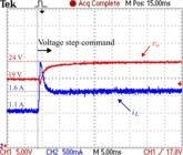
Waveforms of the output voltage and current for the boost converter to verify that it was following the reference voltage.
The experimental results for load disturbance rejection are shown in Fig. 12. As observed, even after adding a resistive load, the converter was able to maintain its output voltage constant at \(19~ ext{V}\) after around \(40~ ext{ms}\) of recovery time. During the transient, the output voltage of the converter decreased by \(3.2~ ext{V}\). It is also important to note that the current had to increase by \(1.2~ ext{A}\) in order to supply the new load configuration.

Load rejection test for the controlled boost converter. Addition of a \(mathbf{30~Omega}\) load in parallel with the existing \(mathbf{39~Omega}\) load.
B. Activation of a permanent magnet synchronous motor
Aiming to represent the robustness of the implemented electronic converter acting as a three-phase inverter, the setup shown in Fig. 9.b was assembled. The PMSM parameters can be viewed in Table 6. A dc power supply Politerm HY3003E-3 was regulated at 10 V and connected to the inverter. Furthermore, it is important to mention that the rotor angular position estimated using the encoder pulses was routed to DAC A, therefore being synthesized at pin J7-70 of the DSP.
In this experiment, the motor was started on a frequency ramp (described in Fig. 13) and the behavior of the system in steady state was analyzed (Fig. 14 and 15). The ramp starting method together with the Volt/Hertz control ensures a gradual increase in the inverter output currents until the end of the machine shaft acceleration. The Volt/Hertz technique is based on the principle that if 50% of the regulated frequency is being supplied, there is also 50% of the voltage at the output. Thereby, at low frequencies, the voltage is also low and, therefore, the current is low. The opposite is also true.

Application of a frequency ramp from 0 Hz to 60 Hz in the reference signal and the consequent responses of the inverter output currents and the angular position of the motor
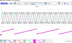

Activation of the protection logic, leading to in the cessation of three-phase currents and the stop of the motor shaft (constant angle signal).
Moreover, Fig. 13 shows the converter output currents \(i_a\), \(i_b\) and \(i_c\), in addition to the angular position of the machine shaft estimated from the encoder pulses. It can be seen that, as the ramp progresses, the inclination of the angular position signal (0 to 2\(\pi\) rad) increases progressively. This indicates that the mechanical speed is also increasing, since the same angular displacement is performed in a shorter time.
The drop in currents when reaching the frequency of 60 Hz, observed in Fig. 13, is due to the fact that, when accelerating, the e.m.f is low. Therefore, the motor demands higher currents. In contrast, when reaching the end of the frequency ramp (steady state), the e.m.f. reaches a value close to the applied voltage, thus the current required to maintain movement is lower than that required to accelerate.
From Fig. 14, it is possible to observe the steady state of the system when the motor reaches the mechanical speed defined by the frequency of 60 Hz. The waveforms of the currents are nearly sinusoidal and has an amplitude of approximately 7 A peak. Similarly, it is noticeable that the period of the angular position waveform is, approximately, 64 ms. This parameter indicates the time required for the motor shaft to make one complete revolution, ranging from 0 to 2\(\pi\) rad. With this time, it is possible to estimate the motor speed using (12).
where \(N_m\) is the mechanical speed (rpm), \(\Delta heta\) is the variation of angular displacement (rad) and \(\Delta t\) is variation of time (s).
In the code developed in PLECS, a protection logic responsible for deactivating the inverter operation in situations of overvoltage or overcurrent was implemented. The maximum voltage and current values delivered to the motor can be adjusted via PLECS. By default, 35 V and 8 A was set. When exceeding these limit, the activation of protection is not instantaneous. This is because it was established that it would only act if the value remains 40 reading cycles above the limit. As the PLECS reading frequency was set at 10 kHz, 40 cycles correspond to 4 ms. Fig. 15 shows the activation of protection during motor operation due overcurrent. In this case, a maximum current of 5 A was set. Therefore, if the system exceeds this protection value for 4 ms, the inverter operation will cease, as is the case. It is noteworthy that the motor shaft stops, since the angular position signal remains constant.
C. Current control of a star-connected RL load
In order to evaluate the performance of the current control loops whose gains were designed in Section III.B and to illustrate the potential of the platform, the load shown in Fig. 9.c was assembled in the laboratory with the parameters in Table 7. The gains were adjusted for bandwidths of 500 Hz and 50 Hz.
Fig. 16 shows the dynamics in synchronous coordinates (dq) for step commands at quadrature axis current and direct axis current at 0.3 ms and 1.8 ms respectively. Both steps with a value of 0.5 A. These data were collected using PLECS Coder interface, showing the behavior of direct and quadrature currents and their references. Since the measured currents are following their references, it is possible to verify that the current loop in Fig. 10 was planned correctly.

Step of 0.5 A in the reference signal and behavior of the (a) quadrature axis current and (b) direct axis current. The controller is set to a bandwidth of 500 Hz.
From Fig. 17, it is possible to observe the impacts of the control in synchronous coordinates of Fig. 16 on the natural variables (a, b and c). For better representation on the oscilloscope, the instants of the steps were changed, but the value and order were maintained, first the quadrature axis current and then the direct axis current. These commands are separated by a time interval of 36 ms. From the step in the quadrature axis current, there is the synthesis of sinusoidal currents at the inverter output with an amplitude of 0.5 A, and with the step in the direct axis current, the amplitude assumes the new value of approximately 0.7 A.

Three-phase currents and direct axis current for a step of 0.5 A on the quadrature axis and then a step of 0.5 A on the direct axis. The controller is set to a bandwidth of 500 Hz.
Fig. 16 and 17 confirm the robustness of the inverter current control system, as it was capable of generating reference currents from commands on direct and quadrature axis currents. Moreover, another notable point of this control is the decoupling between the direct and quadrature axis dynamics, making it possible to regulate and synthesize these parameters independently.
Another analysis developed in this section is the comparison of the bandwidths in the current control. For this, it was applied a quadrature axis current command in step, with a value of 1 A. The direct axis current command was kept at 0. The output currents of the three phases of the inverter as well as the quadrature axis current error are presented in Fig. 18.a and 18.b, for the bandwidths of 500 Hz and 50 Hz respectively. The error signal is due to the fact that the current does not vary instantly in response to the step. Through the controller actions, this error is eliminated during the operation.
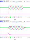
Three-phase currents for a 1 A step in the quadrature axis current, current error (quadrature axis) and the controller with bandwidths of (a) 500 Hz and (b) 50 Hz.
As the system in Fig. 18.b has a bandwidth of 50 Hz, it is noted that it responds more slowly to the step in the quadrature axis current than the one represented in Fig. 18.a, which has a bandwidth of 500 Hz. The times it takes for the controller to extinguish the error are, for the bandwidth of 50 Hz, 10 ms and, for 500 Hz, 2 ms. As expected, the higher the bandwidth, the faster the control and the faster the error approaches zero. However, the initial error is also bigger.
IV. COST ANALYSIS
This paper seeks to defend a more accessible and easily obtainable electronic converter topology. In this context, the LAUNCHXL-F280049C and the BOOSTXL-3PHGANINV are readily available on the market for purchase. In October 2024, the prices of the DSP and the BOOSTXL module are $39.00 (USD) and $49.00 (USD), respectively. Additionally, the unit prices for the motor, inductor, $199.00 (USD), R$130.49 (approximately $22.50 USD), and R$181.47 (approximately $31.30 USD), respectively.
Since this paper proposes a didactic platform, the authors considered that some of the equipment used in the experiments should be made available by the educational institution in a suitable laboratory environment. Among these devices, dc sources, oscilloscope and current probes can be mentioned. Therefore, these costs were not accounted for in this analysis.
VI. DISCUSSIONS
Through the development of this work, it was noted that the proposed platform contributes to the construction of theoretical and practical knowledge in the area of power electronics. In this aspect, the electronic converter topology constituted by the association of the DSP with the BOOSTXL module presents a wide range of possible uses, such as training for students of scientific projects, study material for master and doctoral students, and teaching tool for universities.
The purpose of using this platform in the present work is to provide a training environment for those who participate in research activities, but without excluding the possibility of applying it as a complement to appropriate undergraduate disciplines. Thereby, since the association of DSP with BOOSTXL constitutes an easy-to-program hardware, it can be applied as an experimental verification platform for topologies and control strategies of power electronic converters. Among the possibilities are buck and boost converters and single-phase, three-phase and cascade inverters.
Furthermore, it is worth mentioning that this platform is being applied by the Bat2Grid project (Rede Mineira de Pesquisa e Desenvolvimento em Sistemas de Armazenamento de Energia por Baterias) founded by FAPEMIG. This is a joint action of the following universities: Centro Federal de Educação Tecnológica de Minas Gerais, Universidade Federal de Minas Gerais, Universidade Federal de Viçosa, Universidade Federal de Juiz de Fora, Universidade Federal do Recôncavo da Bahia and Universidade Tecnológica Federal do Paraná.
The experience of Bat2Grid team with this platform started in 2021. Whereas this platform was not in use, each student had to build their own hardware to collect experimental results. This resulted in many prototypes that were not used after the work was completed. In this case, the disposal or reuse of materials was a problem in addition to the physical space required. In this scenario, the proposed platform helps, since it enables the reuse of hardware and the implementation of different projects. Equally, another point that reinforces the training nature of the platform is that some students arrive at research groups with little or no practical experience. In this case, using a lower-cost platform with reduced power makes it easier as well as providing greater safety during the learning phase. Then, if necessary, the student can move on to developing prototypes with higher voltage and power, but already with a complete view of how to perform measurements (current, voltage and position, for example), control and modulation.
VII. CONCLUSION
This study has shown the important role of hands-on learning in power electronics, bridging the gap between theoretical understanding and practical application. When employing a modular educational platform that integrates easily-accessible hardware and user-friendly software, students can effectively engage in experimental work that enhances their comprehension and skills. The detailed hardware setup, comprising the DSP TI C2000 LAUNCHXL-F280049C and the BOOSTXL-3PHGANINV module, offers a versatile and scalable solution for various power electronics applications.
The case studies on the bidirectional boost converter and three-phase inverter illustrate the practical challenges and learning opportunities in real-world scenarios. The results highlight the benefits of experiential learning, such as improved problem-solving skills, increased motivation, and a deeper understanding of power electronics concepts.
Future work could explore different power electronics topologies being implemented in the setup. Additionally, further research could investigate the long-term impact of this hands-on approach on student learning outcomes and career readiness in the power electronics field.
ACKNOWLEDGMENT
The authors thank the support provided by CNPq (Conselho Nacional de Desenvolvimento Científico e Tecnologico), project 408058/2021-8, FAPEMIG (Fundação de Amparo à Pesquisa do Estado de Minas Gerais), projects APQ-0255621 and RED-00216-23, and INERGE (Instituto Nacional de Ciência e Tecnologia em Energia Elétrica). Furthermore, this work was supported by CAPES (Coordenação de Aperfeiçoamento de Pessoal de Nível Superior) - Funding code 001, and the academic excellence program (PROEX).
-
PLAGIARISM POLICY
This article was submitted to the similarity system provided by Crossref and powered by iThenticate – Similarity Check.
REFERENCES
-
1 W. C. Sant’Ana, B. R. Gama, G. Lambert-Torres, E. L. Bonaldi, L. E. L. Oliveira, F. O. Assuncao, D. A. Arantes, I. A. S. Areias, L. E. Borges-Da-Silva, F. M. Steiner, “Development of a Modular Educational Kit for Research and Teaching on Power Electronics and Multilevel Converters”, IEEE Access, vol. 9, pp. 127496–127514, 2021, doi: 10.1109/ACCESS.2021.3112531.
» https://doi.org/10.1109/ACCESS.2021.3112531 - 2 N. Mohan, T. M. Undeland, W. P. Robbins, Power Electronics: converters, applications, and design, 2nd ed., John Wiley & Sons, Inc., New York, N.Y., 1995.
-
3 D. Dujic, A. Cervone, C. Li, P. Bontemps, Y. Frei, “Teaching Power Electronics: How to Achieve the Desired Learning Outcomes?”, IEEE Power Electronics Magazine, vol. 9, no. 4, pp. 45–53, 2022, doi: 10.1109/MPEL.2022.3216094.
» https://doi.org/10.1109/MPEL.2022.3216094 -
4 R. Araújo, H. Teixeira, J. Barbosa, V. Leite, “A hardware tool for explained power electronics control of induction motors”, in 2005 European Conference on Power Electronics and Applications, pp. 8 pp.–P.8, 2005, doi: 10.1109/EPE.2005.219723.
» https://doi.org/10.1109/EPE.2005.219723 -
5 B. S. Dupczak, “Prototipos Did´ aticos para o Ensino Dos Conversores´ CC-CC”, Eletrônica de Potência , vol. 27, no. 3, p. 244–253, Sep. 2022, doi: 10.18618/REP.2022.3.0033, URL: https://journal.sobraep. org.br/index.php/rep/article/view/132
» https://doi.org/10.18618/REP.2022.3.0033» https://journal.sobraep. org.br/index.php/rep/article/view/132 -
6 F. S. Garcia, A. A. Ferreira, J. A. Pomilio, “Plataforma De Ensino De Eletronica De Potência Versˆ atil E De Baixo Custo”,´ Eletrônica de Potência , vol. 13, no. 2, p. 85–90, May 2008, doi: 10.18618/REP.2008.2.085090, URL: https://journal.sobraep.org.br/ index.php/rep/article/view/732
» https://doi.org/10.18618/REP.2008.2.085090» https://journal.sobraep.org.br/ index.php/rep/article/view/732 -
7 M. A. C. Pereira, M. A. M. Barreto, M. Pazeti, “Application of Project-Based Learning in the first year of an Industrial Engineering Program: lessons learned and challenges”, Production, vol. 27, no. spe, 2017, doi: 10.1590/0103-6513.223816, URL: https://doi.org/10.1590/ 0103-6513.223816
» https://doi.org/10.1590/0103-6513.223816» https://doi.org/10.1590/ 0103-6513.223816 -
8 M. Sankey, “Putting the pedagogic horse in front of the technology cart”, , 04 2019, doi: 10.13140/RG.2.2.17755.21288.
» https://doi.org/10.13140/RG.2.2.17755.21288 -
9 I. de los Ríos, A. Cazorla, J. M. Díaz-Puente, J. L. Yague, “Project–based learning in engineering higher education: two decades of teaching competences in real environments”, Procedia Social and Behavioral Sciences, vol. 2, no. 2, pp. 1368–1378, 2010, doi: https://doi.org/10.1016/j.sbspro.2010.03.202, URL: https://www.sciencedirect.com/science/article/pii/S1877042810002429, innovation and Creativity in Education.
» https://doi.org/10.1016/j.sbspro.2010.03.202 -
10 Z. Zhang, C. T. Hansen, M. A. E. Andersen, “Teaching Power Electronics With a Design-Oriented, Project-Based Learning Method at the Technical University of Denmark”, IEEE Transactions on Education, vol. 59, no. 1, pp. 32–38, 2016, doi: 10.1109/TE.2015.2426674.
» https://doi.org/10.1109/TE.2015.2426674 -
11 P. Donoso-Garcia, P. Cortizo, L. Morais, “Ensino Orientado Ao Projeto: Uma Experiencia Para O Ensino De Eletrˆ onica Nas Dis-ˆ ciplinas De Laboratorio De Eletr´ onica E Eletrˆ onica De Potência”,ˆ Eletrônica de Potência , vol. 13, no. 2, p. 109–116, May 2008, doi: 10.18618/REP.2008.2.109116, URL: https://journal.sobraep.org.br/ index.php/rep/article/view/760
» https://doi.org/10.18618/REP.2008.2.109116» https://journal.sobraep.org.br/ index.php/rep/article/view/760 -
12 L. Koleff, L. Araújo, M. Zambon, W. Komatsu, E. L. Pellini, L. M. Junior, “A flexible didactic platform for thyristor-based circuit topologies”, Eletrônica de Potência , vol. 25, no. abr./ju, pp. 154–162, 2020, traduçao. Disponível em: https://doi.org/10.18618/REP.2020.2.0012 Access in: 09 jul. 2024.
» https://doi.org/10.18618/REP.2020.2.0012 -
13 J. V. G. França, J. H. D. G. Pinto, D. d. C. Mendonça, J. V. M. Farias, R. O. d. Sousa, H. A. Pereira, S. I. Seleme Júnior, A. F. Cupertino, “Development of a Didactic Platform for Flexible Power Electronic Converters”, Eletrônica de Potência , vol. 27, p. 225–235, Aug. 2022, doi: 10.18618/REP.2022.3.0012, URL: https://journal.sobraep. org.br/index.php/rep/article/view/73
» https://doi.org/10.18618/REP.2022.3.0012» https://journal.sobraep. org.br/index.php/rep/article/view/73 -
14 J. A. Pomilio, “Atividades Didaticaséxperimentais em Eletronicaˆ de Potencia:ˆ Convergindo Conhecimentos e Tecnologias”, Eletronicaˆ de Potenciaˆ , vol. 25, no. 2, p. 146–153, Jun. 2020, doi: 10.18618/REP.2020.2.0023, URL: https://journal.sobraep.org.br/index.php/rep/article/view/229
» https://doi.org/10.18618/REP.2020.2.0023» https://journal.sobraep.org.br/index.php/rep/article/view/229 -
15 E. A. Vendrusculo, A. A. Ferreira, J. A. Pomilio, “Plataforma Didaticá Para Avaliaçao R˜ apida E Experimental De Estratégias De Controleém Eletronica De Potência”,ˆ Eletrônica de Potência , vol. 13, no. 2, p. 99–108, May 2008, doi: 10.18618/REP.2008.2.099108, URL: https://journal.sobraep.org.br/index.php/rep/article/view/741
» https://doi.org/10.18618/REP.2008.2.099108» https://journal.sobraep.org.br/index.php/rep/article/view/741 -
16 D. Dujic, A. Cervone, R. Barcelos, J. Mace, M. Dupont, “Learning With Your PETS”, IEEE Power Electronics Magazine, vol. 10, pp. 53–61, 12 2023, doi: 10.1109/MPEL.2023.3327669.
» https://doi.org/10.1109/MPEL.2023.3327669 -
17 F. G. Nimitti, A. M. Andrade, “Unraveling Bidirectional Converter Capabilities: a Didactic Platform for Proving Dual-Direction Operation Based on Current Injection”, Eletrônica de Potência , vol. 28, no. 4, p. 287–294, Dec. 2023, doi: 10.18618/REP.2023.4.0020, URL: https://journal.sobraep.org.br/index.php/rep/article/view/159
» https://doi.org/10.18618/REP.2023.4.0020» https://journal.sobraep.org.br/index.php/rep/article/view/159 -
18 CEFET-MG, “Laboratorio de Eletr´ onica de Potência, Acionamentos ê Controle de Processos Industriais.”, Accessed August 3, 2024, URL: https://www.leacopi.cefetmg.br/
» https://www.leacopi.cefetmg.br/ - 19 TI, C2000™ Piccolo™ F28004x Series LaunchPad™ Development Kit, June 2018, user’s Guide.
-
20 TI, “48-V, 10-A, High-Frequency PWM, 3-Phase GaN Inverter Reference Design for High-Speed Motor Drives.”, Accessed August 20, 2024, URL: https://www.ti.com/lit/ug/tiduce7b/tiduce7b.pdf?ts= 1673467385449
» https://www.ti.com/lit/ug/tiduce7b/tiduce7b.pdf?ts= 1673467385449 -
21 TI, “BOOSTXL-3PHGANINV.”, Accessed May 4, 2024, URL: https://www.ti.com/tool/BOOSTXL-3PHGANINV
» https://www.ti.com/tool/BOOSTXL-3PHGANINV -
22 Plexim, “PLECS, The Simulation Platform for Power Electronic Systems.”, Accessed May 4, 2024, URL: https://www.plexim.com/ products/plecs
» https://www.plexim.com/ products/plecs -
23 TI, “TMS320F28004x Real-Time Microcontrollers Guide.”, Accessed July 2, 2024, URL: https://www.ti.com/lit/ds/symlink/tms320f280049c.pdf?ts=1713874244595&refurl=https%253A% 252F%252Fwww.ti.com%252Fproduct%252FTMS320F280049C.
» https://www.ti.com/lit/ds/symlink/tms320f280049c.pdf?ts=1713874244595&refurl=https%253A% 252F%252Fwww.ti.com%252Fproduct%252FTMS320F280049C
-
Associate Editor
Muhammad U. Mutarraf https://orcid.org/0000-0001-7245-2231
-
Editor-in-Chief
Heverton A. Pereira https://orcid.org/0000-0003-0710-7815


 Distribution of LAUNCHXL-F280049C pins and definition of Connection I and Connection II with the BOOSTXL inverter.