 Estimation of nanometer-thickness layer of 6B graphite: an experimental activity to study Ohm’s law in higher education
Abstract
Ohm’s Law is essential for understanding electrical circuits and conductive materials. Formulated by Georg Simon Ohm in the 19th century, it describes the direct proportional relationship between electric voltage and current in ohmic conductors. Despite its apparent simplicity, studies show that students at different educational levels struggle to understand it, mainly due to the abstraction of voltage, current, and resistance concepts. To help overcome these difficulties, this work proposes an experimental activity that applies Ohm’s Law to determine the nanometer-scale thickness of 6B graphite traces deposited on tracing paper. The methodology involves measuring voltage, current, and length, followed by data analysis. The thickness obtained through this approach was compared with results from a Scanning Probe Microscope (SPM). Based on the proposed method, the graphite trace thickness was determined as 456.5(34) nm, while SPM measurements yielded an average thickness of 440(50) nm. The results show good agreement within experimental uncertainties, validating the method’s effectiveness. Therefore, the proposed activity represents a feasible and low-cost alternative for applying Ohm’s Law in undergraduate Electricity courses and, with adaptations, even in high school, helping students connect theoretical concepts with experimental practice.
Palavras-chave:
Teaching of Physics; Ohm’s Laws; Scanning Probe Microscope; Nanomaterials; Graphite on Paper; Electricity
Resumo
A Lei de Ohm é fundamental para a compreensão de circuitos elétricos e materiais condutores. Formulada por Georg Simon Ohm no século XIX, descreve a relação de proporcionalidade direta entre tensão e corrente em condutores ôhmicos. Apesar de sua aparente simplicidade, estudos mostram que estudantes de diferentes níveis de ensino têm dificuldade em compreendê-la, devido à abstração dos conceitos de tensão, corrente e resistência. Para ajudar a superar essas dificuldades, este trabalho propõe uma atividade experimental que aplica a Lei de Ohm para determinar a espessura nanométrica de traços de grafite 6B depositados sobre papel vegetal. A metodologia envolve a medição de tensão, corrente e comprimento, seguida da análise dos dados coletados. A espessura obtida foi comparada a valores determinados por microscopia de varredura por sonda (SPM). Com base na metodologia proposta, a espessura dos traços foi de 456,5(34) nm, enquanto o SPM indicou 440(50) nm. Os resultados mostram boa concordância dentro das incertezas experimentais, validando a eficácia do método. Assim, a proposta representa uma alternativa viável e de baixo custo para o ensino da Lei de Ohm em disciplinas de Eletricidade no Ensino Superior e, com adaptações, também no Ensino Médio.
Keywords:
Ensino de Física; Leis de Ohm; Microscópio de Varredura por Sonda; Nanomateriais; Grafite sobre Papel; Eletricidade
1. Introduction
There is a certain consensus among teachers and researchers in the field of Physics Education regarding the relevance of experimentation as a didactic approach [1]. Studies such as that of Parreira and Dickman (2020) show that both instructors and students in engineering programs unanimously recognize the importance of physics experiments in stimulating greater student participation in academic activities, as well as in significantly contributing to the consolidation of theoretical concepts through their practical application [2]. Moreover, the students who participated in that study also highlighted how experimental practices help relate the studied theories to everyday life [2].
Indeed, the use of didactic experiments in science education plays a fundamental role in student learning. Through hands-on practice, motivated by curiosity, students can explore new knowledge, raise questions about different topics, and develop more meaningful learning [3]. Experimental practice also enables them to connect theory to everyday experience in a practical way, encouraging reflection and the expression of ideas [3]. Considering students’ prior knowledge, experimental practices can aid in the assimilation of new concepts, given that the practical aspect of the activity may serve as an engaging factor [3]. This type of experimentation relates to David Paul Ausubel’s Theory of Meaningful Learning, which proposes that students assign personal meaning to what they learn by connecting new information to their existing knowledge. When this connection does not occur, learning becomes mechanical, without real integration into the cognitive structure. In such cases, knowledge is memorized without deep understanding [4].
Experimental activities tend to stimulate active participation, arousing curiosity and making learning more engaging and motivating [5]. Thus, they become an effective strategy to overcome difficulties, fostering knowledge construction and the development of scientific skills [5]. Furthermore, as pointed out by Carrascosa (2006) [6], it is important to design experimental activities with an investigative character, avoiding overly rigid scripts that could limit reflection and creativity, as if they were mere step-by-step recipes to be followed mechanically.
Ohm’s Law presents itself as a highly abstract mathematical relationship for students, requiring different approaches to consolidate its meaning. In the literature, various studies employ experimental practice to address Ohm’s Law. The study by Prastyaningrum & Pratama (2019) [7] investigated students’ conceptions of Ohm’s Law using a qualitative method, collecting data through open-ended questions and interviews. Analysis of the results revealed that electrical engineering students do not fully understand the concept of Ohm’s Law, mainly due to difficulties in interpreting the language of physics applied to electrical phenomena. The study also emphasized the importance of project-based teaching as a strategy to reduce misconceptions and enhance understanding of the fundamentals of electricity.
Other studies – such as Rocha & Santiago (2017) [8] and Oliveira (2015) [9] approach Ohm’s Law by determining the resistance and/or resistivity of materials based on the analysis of electrical circuits and the use of devices such as ammeters, voltmeters, power supplies, and resistors. Similarly, Santos & Dickman [10] used real experiments with circuits composed of power sources and resistors, along with virtual simulators.
Alternative approaches can also be found in the literature. Vasconcellos (2024) [11] explores Ohm’s Law through analogies between hydraulic and electrical phenomena. Baião, Amaral & Veraszto (2017) [12] present a methodology involving the use of Arduino combined with the Scratch software. Castro (2019) [13] conducted a similar activity entirely virtually using Scratch. Domingos & Teixeira (2022) [14] employed a PhET simulator to teach the law. The use of simulators in distance education contexts was also investigated by Silva & Duarte (2023) [15].
Strategies and methodologies to approach the topic in more inclusive ways are also found in the literature. For example, Velloso et al. (2021) [16] developed activities through Cooperative Learning at the higher education level for visually impaired students.
Several other works apply Ohm’s Law to the measurement of physical quantities in graphite layers from pencils, both for pedagogical purposes and for experimental measurements. Activity proposals for quantifying the thickness of graphite on paper have been described for high school [17], though without appropriate statistical treatment consistent with higher education. Rocha Filho et al. [18] proposed an activity for analyzing and calculating the electrical resistance of series and parallel resistor combinations made with multiple heavy pencil strokes using soft graphite (type 6B) on sulfite paper for high school education, emphasizing experimental learning in electricity with the aid of a multimeter. Vilela and Pereira (3) developed a similar proposal, also aimed at high school students. One of their conclusions was that the profilometry technique used to investigate the thickness of the graphite traces was not an effective or precise solution, as the roughness of the paper on which the graphite was deposited was already on the same order of magnitude as the graphite layer’s thickness [19]. Moraes et al. (2025) [20] developed a playful classroom activity on Ohm’s law using simple materials such as graphite-coated paper strips and analog multimeters, integrating theory and experimentation to enhance students’ understanding of electric circuits. Evangelista et al. (2024) [21] reported an experimental classroom activity that related the proportionality between resistivity, area, length, resistance, voltage, and electric current. Using 6B graphite traces on graph paper as adjustable resistors, students built a lighthouse prototype with LEDs controlled by Arduino to visualize electrical behavior and basic programming logic.
Studies analyzing aspects associated with graphite deposited on paper illustrate other applications and potentialities related to the proposal presented here. Santiago et al. (2017) demonstrated that layers of graphite from 4B pencils (General’s Pencil Company, NJ, United States) manually deposited on wax-treated paper can be used for the simple and rapid fabrication of high-performance electrochemical sensors [22]. Srinivas and Kumar compiled studies on the application of pencil graphite electrodes as dopamine sensors [23]. Their review highlights the use of pencil graphite electrodes (PGE) as an accessible and efficient alternative for electroanalytical applications, emphasizing their usefulness in teaching electrochemical concepts. Although PGEs require surface treatment for activation due to their initially electro-inactive nature, they prove effective for the sensitive detection of dopamine, a common model compound in studies. Thus, the research indicates that properly treated PGEs offer a low-cost, highly selective tool for educational experiments, enabling the introduction of electrochemical techniques and compound analysis in the classroom. The review also suggests that future research on surface functionalization and dopamine analysis in the presence of other analytes could further expand their applicability in educational and research contexts.
Dhanabalan, Chua, and Ricardo [24] developed a comprehensive study on the properties of layers of different graphite grades (B to 8B) from pencils applied as electrodes on paper, evaluating how certain variables can influence the resistance of deposited graphite electrodes: the deposition direction relative to the potential difference, the length and cross-sectional area of the deposited layers, the number of layers deposited, the duration of potential application, and the graphite type.
Grisales et al. (2016) [25] presented a simple and low-cost method for producing graphite-based conductive ink and applying it to the construction of electrical circuits on paper for pedagogical use. The ink exhibited ohmic behavior and allowed the creation of resistors and parallel-plate capacitors with different geometries. The results indicate that activities using conductive ink represent an effective didactic tool for teaching electricity and electronics, enabling experimental visualization of the relationship between resistance, capacitance, and geometric factors in circuits.
Considering the reviewed literature, this study aims to propose an experimental activity for higher education courses in Electricity. The proposal investigates the application of Ohm’s Law in measuring the nanometric thickness of graphite traces using, among other tools, the scanning probe microscopy (SPM) technique. Moreover, the ease of assembling the experiment promotes greater student engagement [2] and aligns with a more investigative approach [6].
Specifically, the development of the proposed activity aims to provide students with a deeper conceptual understanding of Ohm’s law and electrical resistivity by relating theoretical expressions to experimentally measurable quantities. The activity is designed to foster practical skills in experimental data acquisition, uncertainty analysis, graphical representation, and linear fitting, emphasizing the interpretation of current–voltage relationships and resistance as a physical property. In addition, the proposal highlights the use of indirect measurement procedures to estimate quantities that are not directly accessible, such as the nanometric thickness of graphite layers, thereby promoting students’ awareness of measurement scales and the role of modeling and approximations in experimental physics.
The following sections focus on a theoretical review of Ohm’s Law and on some properties of graphite, the material used in the experiment.
2. Ohm’s Law
The electric current flowing through a material, due to a potential difference between two points, may behave differently depending on the type of material, even under the same conditions of voltage, electrical contact area, and path length along the material. It is known that electric current can depend on several other factors such as temperature, pressure, physical state, and the composition of the material (pure or mixed). However, despite the various factors that can influence the conductive capacity of materials and the different relationships between the applied potential difference (V) and the electric current (I), there is a simpler case in which these two quantities are directly proportional [26]:
In this case, the proportionality constant, denoted by R, is called the electrical resistance. It is interpreted as the opposition a medium exerts on the movement of electric charges (electric current) under the action of a potential difference. Thus [26]:
The mathematical expression above is attributed to the German scientist Georg Simon Ohm (1789–1854), who conducted studies in this field, and it became known as Ohm’s Law [27]. The unit of measurement for electrical resistance is defined as the ratio between the electric potential difference and the electric current, that is, volts per ampere (V/A), designated as the ohm (W) in honor of the German scientist [28].
It is also possible to define a vector quantity involving the electric current in a three-dimensional region, known as the current density, denoted by the vector (“J” vector). There is a vector equivalent of Equation (2) that involves , defined as [29]:
Where is called the conductivity of the medium, measured in siemens per meter (S/m), and is the applied electric field, measured in newtons per coulomb (N/C) or volts per meter (V/m). The conductivity of the medium is an intrinsic property of the material and refers to its ability to conduct electric current. From the conductivity of the medium, another physical quantity can be defined, its inverse, known as the resistivity () [29]:
Its unit of measurement is defined as ohm-meter () [29]. The values of determine the classification of materials according to their electrical conductivity: values between and are considered conductors, typical of metals and metal alloys; values between 5, and 3, are considered semiconductors; and values above the order of are considered insulators [30].
The relationship between electric current and current density can be established by the following Equation [31]
Where is an infinitesimal surface element, whose direction and orientation are defined by the vector normal to the surface, with a magnitude equal to the area. Figure 1(a) a illustrates Equation (5).
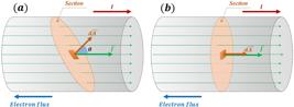
Representation of the relationship between electric current, current density, and oriented surface for two different situations: (a) when and are not parallel; (b) when and are parallel.
For a specific situation in which is parallel to the infinitesimal elements (Figure 1(b)), it can be considered that [31]:
In which the integral of the infinitesimal area element equals the area of the surface over which the flux is analyzed.
To obtain another important relationship regarding the resistance and resistivity of a material, consider a cylinder with a cross-section of area A and length L, made of a material with conductivity . Assuming that the potential is constant and homogeneous at its ends, forming an electric field perpendicular to the cross-sectional area, the magnitude of Equation (3) can be related to (Equations 3) and (6) as follows:
Knowing that the electric field can be defined in terms of the potential difference (V) and the path (L) over which the electric field extends parallelly [32]:
Thus, by substituting (Equations 4) and (8) into Equation (7) and expressing V as a function of I [29, 32]:
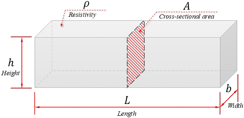
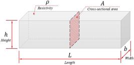
By comparing Equation (9) with Equation (1), one can establish a relationship for the resistance of a material as a function of its geometric properties – such as length (L) and cross-sectional area (A) – and its compositional property, resistivity (), schematically represented in Figure 2. Thus [32]:
For more detailed derivations and discussions, the books by Kleber Daum Machado [28] and David J. Griffiths [29] are recommended.
It is worth noting that, in high school physics textbooks and classes, the relation given by Equation (10) is commonly referred to as Ohm’s Second Law, while Equation (2) is usually called Ohm’s First Law.
Materials that exhibit a linear relationship between the applied electric voltage and the electric current are called ohmic materials, whereas a non-ohmic material displays a nonlinear relationship between these two quantities [30].
3. The Properties of Graphite
Graphite is a stable form of carbon under ambient temperature and pressure conditions. Its crystalline structure is composed of parallel planes formed by carbon atoms arranged at the vertices of interconnected regular hexagons. Within these planes – referred to as layers or lamellae – each carbon atom is bonded to three coplanar neighbors through sp2-hybridized orbitals. It is worth noting that each individual layer corresponds to graphene, a carbon nanomaterial with exceptional properties. The first graphene sample was obtained by the successive separation of layers from a piece of graphite using adhesive tape until only a single layer of carbon atoms remained. This method, known as micromechanical exfoliation or the “scotch tape technique”, was one of the earliest approaches that allowed the production of high-quality graphene. The characteristic hexagonal configuration of the sp2 bonds can be seen in Figure 3. Furthermore, the fourth valence electron of each carbon atom is not confined to a specific bond but is instead delocalized, contributing to a molecular orbital that extends throughout the structure and lies between the layers. The interactions between these layers occur perpendicularly to the planes, along the crystallographic c-direction, as shown in Figure 3, and are of the van der Waals type – relatively weak forces that hold the lamellae together [30].

Graphite exhibits both metallic and non-metallic characteristics, making it a valuable material for the manufacture of electrodes [34]. In its pure form, graphite has a resistivity ranging from to [30]. Graphite pencils are produced from a combination of materials, in which fine graphite powder is incorporated into a matrix that may be inorganic, such as resins, or organic, including clay or high–molecular-weight polymers like cellulose [35]. In general, graphite pencils are composed of approximately 65% graphite, 30% clay, and a small fraction of binding agents, such as waxes, resins, or polymers [36]. According to the established European grading scale, graphite pencils are categorized by letters and numbers based on their composition: the letter H denotes hardness, indicating a higher clay content that makes the pencil harder, while the letter B represents blackness, corresponding to a higher graphite content that makes the pencil softer and darker. The gradation scale ranges from 9H (the hardest) to 9B (the softest), with HB pencils consisting of a balanced ratio of graphite and clay [37, 38, 39, 40, 41]. The presence of clay in the pencil composition directly influences both its chemical properties, such as ion-exchange capacity, and its structural characteristics, including the degree of disorder and surface morphology [39].
Due to its crystalline structure, graphite exhibits properties that are strongly associated with anisotropy, meaning that its properties vary depending on the crystallographic direction in which they are measured. Regarding its electrical properties, the electrical resistivities parallel and perpendicular to the graphene planes, layers, or lamellae are on the order of and , respectively. This behavior can be explained by the high mobility of free electrons in graphite, whose movements are more favorable when subjected to an electric field applied parallel to the planes, resulting in relatively low resistivity in that direction [30]. Furthermore, due to the weak van der Waals forces between the layers, the planes can easily slide over each other, which gives graphite its excellent lubricating properties [30] and explains its use in writing pencils. Mechanically, graphite is very soft and brittle, possessing a relatively low modulus of elasticity compared to diamond, another carbon polymorph. Its electrical conductivity in-plane is to times higher than that of diamond, while its thermal conductivity is practically the same. The coefficient of thermal expansion of graphite is small and negative in-plane, whereas it is positive and relatively large perpendicular to the planes, in contrast to diamond, which has a small and positive thermal expansion coefficient. Optically, graphite is opaque and exhibits a black-silver coloration [30].
Other important properties of graphite include good chemical stability at high temperatures and in non-oxidizing atmospheres, high resistance to thermal shock, strong gas adsorption, and good machinability. Due to its diverse properties, graphite has a wide range of applications, such as: lubricants, battery electrodes, friction materials (e.g., brake pads), heating elements for electric furnaces, welding electrodes, metallurgical crucibles, refractories and high-temperature insulators, rocket nozzles, chemical reactor vessels, electrical contacts, and air purification devices [30].
4. Materials and Methods
The methodology used was divided into five subsections: determination of the resistivity of 6B graphite; deposition of a graphite layer on tracing paper; measurement of the average width of the graphite layer; determination of the thickness of the deposited graphite layer; and measurement of the average thickness of the graphite layer using SPM.
4.1. Materials
For the resistivity measurements of graphite, the following materials and equipment were used: a Faber-Castell Castell 9000 6B hexagonal graphite pencil, Canson A4 tracing paper (60 g/m2), Chamex white A4 office paper (75 g/m2), utility knife, polished granite slab for support, 30 cm millimeter ruler, ballpoint pen, two POL-79C Dual Display bench multimeters, Instrutherm FA-3050 symmetrical digital 2-channel power supply, two banana plugs, two alligator clips, Marberg digital caliper (0–200 mm), two three-finger clamps with fixed ferrules, two simple double ferrules, universal support, plastic clipboard, and Shimadzu SPM-9700HT scanning probe microscope.
4.2. Methods
4.2.1. Determination of the resistivity of 6b graphite
The measurement system was assembled as shown in Figure 4.

(a) Schematic of the setup for measuring resistivity. (b) Representation of the electrical circuit used for the measurement.
Initially, the ends of the pencil were sharpened using a utility knife. Using a digital caliper, ten measurements of the diameter were taken on each end of the graphite, totaling 20 measurements. These values were used to calculate the average diameter of the graphite and, consequently, the cross-sectional area through which the electric current flowed. On both ends, the pencil was shaved with the utility knife and scratched onto an A4 office paper sheet (75 g/m2, Chamex white) placed on a smooth surface, in order to obtain a flat face as perpendicular as possible to the pencil’s longitudinal axis. Next, the caliper was used to measure the longitudinal dimension of the graphite, considered as its length (L). Banana-type plugs were positioned at the ends of the graphite to serve as electrical terminals for the power supply and the multimeter set in ammeter mode. A significant pressure was applied between the plug and the graphite, and it was verified that current could pass. The voltmeter terminals of the multimeter were connected to the graphite ends using alligator clips, which were then connected to the voltmeter. With the system assembled as shown in Figure 5, the electric currents passing through the graphite were measured as the voltage across the terminals was gradually increased.

(a) Photograph of the experimental setup used. (b) Photograph showing the contact of the plugs with the pencil graphite. (c) Photograph showing the contact of the ammeter and voltmeter plugs with the graphite. (d) Photograph showing the contact of the banana-type plug with the cross-section perpendicular to the longitudinal axis of the graphite.
For the study of the physical quantities involved in the experiment, it was more consistent to rewrite Equation (9) with I as a function of V, since the electric current through the material varies according to the potential difference applied across the pencil terminals:
Thus, the least squares method can be used to obtain a linear function that describes the relationship between the quantities involved in Equation (12):
Where a is the slope, b is the intercept, and x is the independent variable. Comparing this with Equation (11), it can be seen that a is associated with the applied voltage (V), while the intrinsic physical quantities of the material – cross-sectional area, length, and resistivity – act as the slope (a) of the linear function, and f(x) corresponds to the current (I), which depends on V. The intercept (b) should be close to zero, since the quantities are directly proportional. Thus, the resistivity of 6B graphite can be obtained from the following relation:
Isolating :
The obtained value of r will be used in the next step, described in the following section.
4.2.2. Deposition of the graphite layer on tracing paper
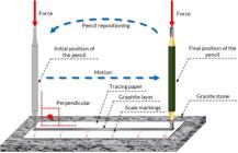
The graphite layer was deposited using the same graphite as in the previous section on Canson A4 60 g/m2 translucent tracing paper, supported on a polished granite slab. The deposition was performed with the pencil held perpendicular to the paper, applying sufficient hand pressure to produce a continuous and homogeneous stroke, as shown in Figure 6. A total of 50 layers were deposited using a single-direction movement of the pencil; that is, upon reaching the end of the stroke, the pencil was lifted and repositioned at the starting point to continue in the same direction. This approach is strongly recommended to ensure film uniformity, as it minimizes local thickness variations, prevents irregularities caused by graphite accumulation when reversing the motion, and improves the consistency of the electrical resistance along the measured length. It is recommended to make a stroke 12 cm long, 2 cm longer than the 10 cm that will be used for measurements. To assist in subsequent measurements, markings from 0 to 10 cm, spaced every 2 cm, were made using a 30 cm millimeter ruler (error: 0.05 cm) and a ballpoint pen. It is worth noting that a quick empirical test to evaluate the effectiveness of the deposition consists of holding the sheet up to a light source and checking whether the light passes easily through the graphite layer.
4.2.3. Measurement of the average width of the graphite layer
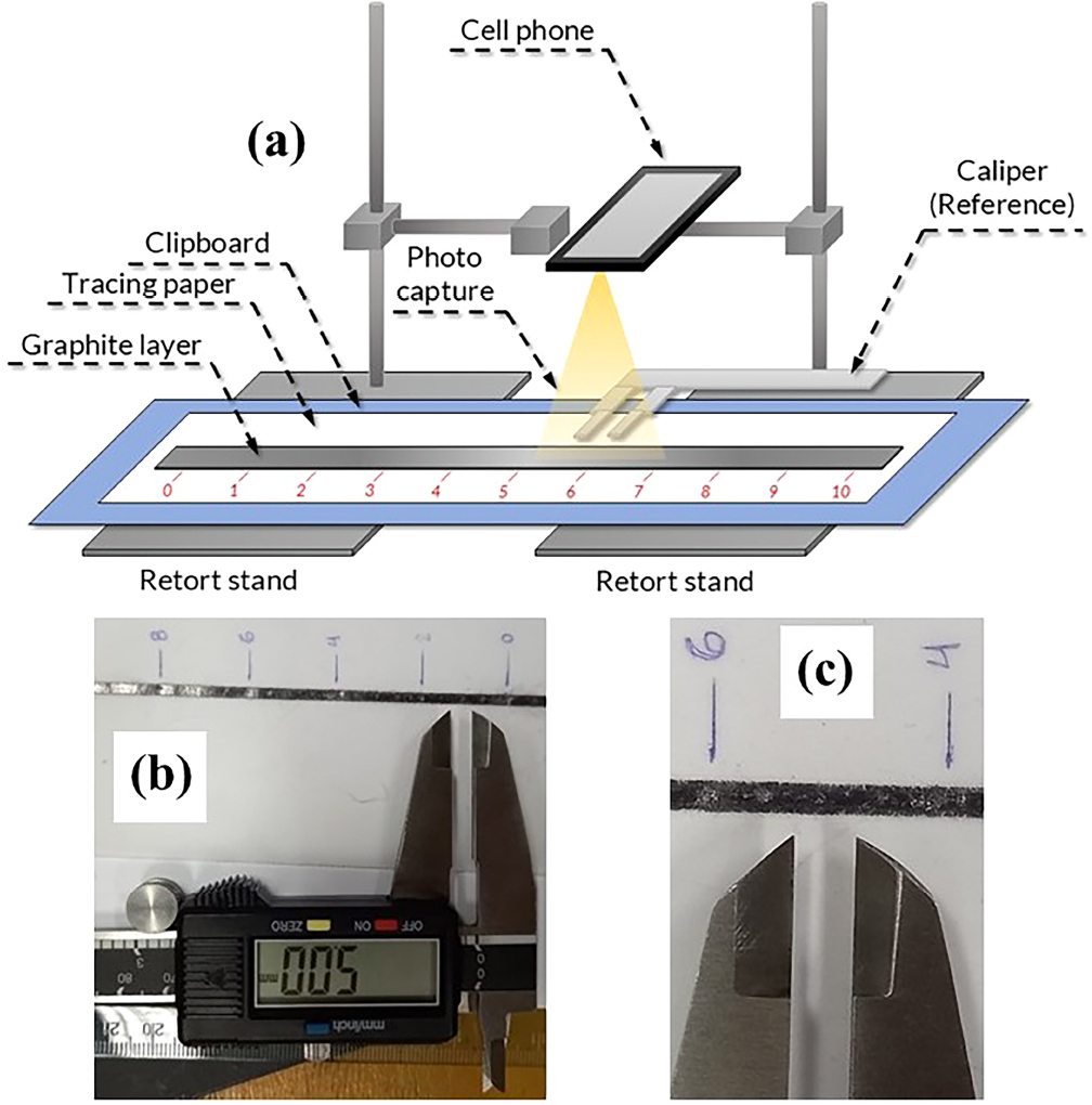
The measurements of the width of the graphite layer deposited on the tracing paper, also referred to as the width (letter b) in Figure 2, were performed using the rear camera of a Samsung A12 smartphone with a resolution of pixels. The smartphone was positioned above the graphite layer using a universal support with the aid of clamps. The widths of the graphite stroke along its length were measured using the ImageJ software, taking as reference a Marberg caliper opened to 5.00 mm, placed near the graphite layer. Fifty measurements were taken for each of the different segments: 0–2 cm, 2–4 cm, 4–6 cm, 6–8 cm, and 8–10 cm. Figure 7(b) and (c) show examples of the images collected.
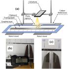
(a) Schematic of the experimental setup for capturing images of the graphite layer. (b) Marberg caliper positioned near the deposited graphite layer. (c) Zoomed-in view of the 4–6 cm region of the graphite layer, according to the previously marked graduations.
4.2.4. Determination of the thickness of the deposited graphite layer
The thickness of the graphite can be determined using the relationships developed in the “Ohm’s Law” section. The cross-sectional area of the graphite layer can be approximated as a rectangle with width b and height h, where h is the quantity to be determined, in this case, the thickness of the graphite layer, as shown in Figure 2. The product of b and h gives the cross-sectional area (A); thus, using Equation (3):
Measurements of the electric current (I) passing through the graphite layer were performed as a function of the applied potential difference (V) at its terminals for different values of L: 2, 4, 6, 8, and 10 cm, according to the auxiliary graduations marked on the paper. The distances were adjusted relative to the spacing between the two banana-type plugs in contact with the central graphite layer, positioned away from the transverse edges to maintain greater homogeneity in the measurement, since the edges may have a lower deposition of graphite layers. Figure 8 shows the schematic of the measurement system setup, and Figure 9(a) shows the actual setup. Figure 9(b) illustrates the circuit diagram, in which the graphite layer functions as a potentiometer due to the variation of its resistance with the measured length. To improve the contact between the graphite layer and the plugs, a sheet of A4 office paper (75 g/m2, Chamex white) was inserted under the tracing paper. Figure 9(c) and (d) show the actual setup, with Figure 9(d) detailing how the contact between the plug and the graphite layer was made.


(a) Electrical circuit representing the measurement system. (b) Scheme for electrical measurements on the graphite layer deposited on tracing paper. (c) Detail of the connection of the banana-type plugs with the graphite layer deposited on tracing paper. (d) Detail of the contact between the banana-type plug and the graphite layer deposited on tracing paper.
The value of to be used is the one obtained in the first experimental stage. Thus, the thickness h can be determined by comparing Equation (15) to a linear function, Equation (12), and again applying the least squares method to obtain the coefficients of the linear function, which are:
With the value of L properly applied for each experimental measurement performed at a given length L, the five sets of measurements obtained according to the methodology described in the section “4.2.3. Measurement of the average width of the graphite layer” can be used to determine h by isolating this quantity:
Since the graphite layer is neither perfectly smooth nor has a rectangular cross-section, the obtained value represents only an approximation, considering the layer as a parallelepiped shape. Thus, from the different values of h determined for various lengths L, the arithmetic mean of h can be calculated to estimate a representative value of the average thickness of the graphite layer along its entire length.
4.2.5. Measurement of the average thickness of the graphite layer using SPM
The thickness measurements of the deposited graphite layers were performed using a Shimadzu SPM-9700HT scanning probe microscope (SPM) available at a partner institution, with instrumental errors of 0.2 nm in the xy scanning plane and 0.01 nm in height (z-axis). The analysis was conducted using a non-contact type tip to measure the topographic distribution at the interface between the tracing paper and the graphite. The images were processed using the open-source software Gwyddion, version 2.68. The values obtained with the SPM were then compared with the values calculated based on Ohm’s Law and those obtained in the previous experimental steps.
The measurement of the graphite layer thickness at the paper interface was conducted with the aid of an optical microscope attached to the AFM sample holder to locate a representative transition region between the graphite and the paper. Once this region was identified, the AFM scan was aligned accordingly, and a m topographic image was acquired using the non-contact tip. The images were then processed with Gwyddion to determine the thickness by extracting height profiles from regions of interest.
5. Results
The data, equations, and error propagation procedures employed in the statistical analysis are available in the Supplementary Material.
5.1. Determination of the resistivity of 6b graphite
According to the methodology described, the average diameter of the pencil graphite was measured, yielding a value of m and, consequently, a cross-sectional area of (see Supplementary Information, Section A). The length of the pencil graphite was measured as m. Figure 10 shows the graph of current versus applied voltage for the graphite. The high goodness of fit (R2 = 0.99787) demonstrates that, within the investigated voltage range (0–3.2338 V), graphite exhibits an ohmic behavior, as evidenced by the linear current–voltage response. Accordingly, the relationship obtained from the least squares fitting is given by1:
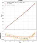
In this case, the slope (a) was A/V, the intercept (b) was A, and the coefficient of determination (R2) was 0.99787. Using these values and performing the appropriate error propagation, the resistivity of the pencil graphite was calculated from Equation (14), yielding ., which differs from the expected value for pure graphite (5, to 3,) due to the presence of other substances in its composition (see Supplementary Information, Section B).
Although the I–V characteristics are predominantly linear over the investigated voltage range (R), a slight systematic curvature is observed in the residuals together with a small non-zero intercept. This behaviour suggests the presence of weak second-order contributions, which may be attributed to contact resistance and to Joule heating at higher voltages. At the highest applied bias ( V) and current ( A), the dissipated power reaches W, which can induce a modest temperature rise of the graphite and consequently a small variation of its resistivity. Nevertheless, these effects remain minor compared to the dominant ohmic response, and the resistivity values extracted from the linear fits are unchanged within experimental uncertainty when the analysis is restricted to the low-voltage regime.
5.2. Deposition of the graphite layer on tracing paper
After depositing the graphite layers on tracing paper following the methodology described in the section “Deposition of the Graphite Layer on Tracing Paper”, the widths (b) of the deposited graphite layers were measured, yielding different values for the selected segments, as shown in the table below:
Fifty measurements were taken for different segments of the deposited graphite. That is, for the segment “0–2 cm”, 50 width measurements were obtained; for the segment “2–4 cm”, another 50 measurements were taken, and so on up to the segment “8–10 cm”. The data were then aggregated for statistical analysis as the length increased (see Supplementary Information, Section C). For example, the length “0–6 cm” includes all data from the segments “0–2 cm”, “2–4 cm”, and “4–6 cm”, totaling 150 measurements, since it comprises three segments. The values presented in Table 1 were used in the calculations described in the following section.
Values obtained for the width measurements of the graphite layer deposited on tracing paper.
Fifty measurements were performed for each segment of the graphite layer (0–2 cm, 2–4 cm, 4–6 cm, 6–8 cm, and 8–10 cm) to ensure statistical reliability and to capture possible local variations along the layer. This extensive sampling was considered sufficient to provide a representative assessment of the layer properties, although it does not preclude the use of a different number of measurements.
5.3. Determination of the thickness of the deposited graphite layer
Using the values of resistivity (ρ) and the width (b) of the graphite layer deposited on the tracing paper, obtained from the methodologies described previously, it was possible to estimate the thickness of each deposited layer for the different lengths, using the slope obtained from the linear fit, according to Equation (17). The relevant values are presented in Table 2. The plot, along with the linear fit using the least-squares method and the residuals, corresponding to the “0–10 cm” section is shown in Figure 11, while the remaining plots and calculation details are provided in Sections D and E of the Supplementary Information.
Measurements of the thickness of the graphite layer deposited on tracing paper for different reference lengths Note that the slope a of the linear fit corresponds to . For the calculation of the layer thickness, the value of obtained in Section 5.1 was used.
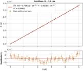
Current–Voltage (I–V) curves obtained for the graphite layer deposited on the substrate over the 0–10 cm section.
The variation in layer thickness with reference length reflects natural fluctuations in the graphite trace along the paper, including small differences in deposition and the inherent irregularity of the substrate (Canson A4 60 g/m2 translucent tracing paper). It is important to emphasize that the thickness values reported in Table 2 should be interpreted as effective thicknesses, derived from a simplified geometrical and electrical model, as illustrated in Figure 2. The analysis assumes a uniform rectangular cross-section for the graphite trace and a homogeneous, isotropic resistivity equal to the effective resistivity measured for the deposited graphite–binder composite. However, graphite is intrinsically anisotropic, and the manual deposition process is expected to introduce local variations in width, thickness, packing density, and orientation of graphite flakes along the trace. Consequently, the resistivity and cross-sectional area may vary spatially, leading to systematic deviations from the idealized model.
In this context, the proposed approach does not aim to provide a local or absolute measurement of the graphite layer thickness, but rather an average effective thickness that captures the combined electrical and geometrical response of the deposited layer over the analyzed length. This simplification is intentional and aligns with the didactic objective of the activity, allowing students to explore indirect measurement, modeling assumptions, and sources of uncertainty in a realistic experimental setting.
5.4. Measurement of the average thickness of the graphite layer using SPM
From the SPM analyses, images were obtained showing the presence of steps at the interface regions between the deposited graphite layer and the tracing paper. One representative SPM image is shown in Figure 12, while the other two are presented in Section F of the Supplementary Information.

SPM figure obtained from spm analyses: (a) Two-dimensional image, with the blue dashed rectangle indicating the area from which the average height profile was extracted; the arrow shows the direction corresponding to the graph, with the start of the arrow at the left side and the tip at the right side of the graph. (b) Three-dimensional image. (c) Average height profile of the region highlighted in the two-dimensional image.
From the data obtained through scanning probe microscopy (SPM) analysis, it was possible to extract height profiles from regions of interest, with the data presented in the Supplementary Information, Section G. The regions from which the profiles were extracted are highlighted by blue dashed rectangles in the two-dimensional images (Figure 12(a)). Arrows indicate the profile direction, with the left side corresponding to the arrow origin and the right side to its endpoint. To obtain statistically meaningful measurements, the average height of each selected region was calculated, and the step height was determined as the difference between this average value and the lowest point of the step, taken as the step base. In the height profiles (Figure 12(b)), the components are indicated as follows: the profile data are shown in blue, the step bases as pink dashed lines, the average step height as a green dashed line, and the step limits as red dashed lines. The thickness of the deposited graphite layer was defined as the difference between the “Base” and the “Average Height” lines. The step values obtained from the SPM analysis are presented in Table 3.
Due to the inherent roughness and malleability of the tracing paper, the deposition of the graphite layer does not produce a perfectly sharp step. To obtain representative thickness values, an optical microscope was used to identify a transition region between the graphite track and the paper, which was then aligned with the AFM scan. Despite these limitations, this approach allows reliable determination of the average layer thickness
5.5. Comparison between method
The measured value obtained using the proposed method, 456.5(34) nm, shows good agreement with the 440(50) nm measured by AFM, which serves as the direct reference. The uncertainty interval of the proposed method (453.1–459.9 nm) lies well within the broader AFM interval (390–490 nm), indicating substantial overlap and compatibility between the two approaches. The difference between the mean values, 16.5 nm, corresponds to approximately 3.8% of the AFM value, emphasizing that the deviation of the proposed method from the reference is small.
Considering the combined uncertainty of this difference, calculated as the quadratic sum of the individual uncertainties ( nm), the resulting interval (34 to 66 nm) includes zero, confirming that the difference is not statistically significant. The relatively small uncertainty of the proposed method reflects the high internal consistency of its measurements, although it does not capture all sources of experimental variability considered by AFM. These results indicate that the proposed method produces measurements consistent with direct AFM observations within experimental uncertainty. Figure 13 presents a graphical comparison, highlighting the agreement between the proposed methodology and the reference measurements.
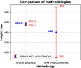
Comparison of the proposed methodologies used in the present study: using electrical measurements and using scanning probe microscopy (SPM) measurements.
It is worth emphasizing that the uncertainty associated with the average graphite layer thickness obtained by SPM is greater than the uncertainties obtained through the methodology proposed in the present article. This result arises from the combination of statistical dispersion among the measured values and the limited number of independent measurements (three analyzed profiles). While the uncertainties reported for each individual step height (500(17), 819(19), and 363(8) nm) are predominantly determined by instrumental resolution and profile analysis, derived from the standard error of the mean of each height profile and the propagation of the SPM vertical uncertainty (0.01 nm), the uncertainty of the weighted average additionally incorporates the variability between these distinct measurements. As presented in Table S23, the significant spread among the individual values leads to an increased uncertainty in the final averaged thickness (440(50) nm), reflecting the overall heterogeneity of the deposited graphite layers. It should also be noted that acquiring high-quality SPM images suitable for reliable thickness determination is experimentally demanding and time-consuming, and the selected profiles result from careful analysis following extensive exploration. Therefore, the reported uncertainty of the average should be interpreted as a realistic estimate that accounts for both measurement precision and sample variability. The complete methodology for uncertainty propagation is detailed in Section G of the Supplementary Information.
6. Conclusion
This work presented an experimental approach for estimating the thickness of 6B graphite traces through electrical measurements based on Ohm’s Law, complemented by direct measurements obtained via scanning probe microscopy (SPM). The indirect electrical method yielded a thickness of approximately 456 nm, while the direct SPM measurement indicated a value close to 440 nm, with overlapping uncertainties. This agreement demonstrates that fundamental electrical relations, when combined with careful experimental design, can provide reliable nanometric-scale estimations using relatively simple and accessible instrumentation. In contrast to the direct topographical characterization provided by SPM, the proposed method relies on macroscopic electrical measurements to infer thickness, highlighting its pedagogical value by connecting microscopic structural parameters to measurable electrical quantities.
The results validate the proposed methodology as a viable and accessible alternative for estimating the thickness of graphite layers in educational contexts. The experiment integrates theoretical and practical aspects of Electricity, enabling students to relate resistivity, geometry, and current–voltage behavior within a coherent framework. Its relative simplicity makes it particularly suitable for undergraduate laboratory activities. For high school implementation, adaptations may include the use of predefined trace lengths, controlled geometrical templates, and previously determined resistivity values, thereby simplifying calculations while preserving the conceptual connection between resistance and material properties.
Some limitations of the present approach must be acknowledged. Surface roughness may contribute to variations in the effective thickness and should be systematically evaluated in future studies. Similarly, implementing a controlled deposition setup that specifically regulates the pressure applied by the pencil during graphite deposition would likely improve reproducibility and reduce thickness variability. However, such an implementation would increase experimental complexity and was not incorporated in the current study. This aspect is identified as a potential refinement for subsequent investigations.
The lower applicability limit of the proposed approach is dictated by both the morphological and physical characteristics of ultrathin graphite deposits. Graphite exhibits particles with a flake-like morphology [42], and in very thin deposits it forms an inherently discontinuous layer. As a result, electrical conduction is governed by percolation pathways [43] rather than by a well-defined and continuous film thickness. In this regime, the classical relation between resistance and thickness ceases to hold, making any inferred thickness largely meaningless. Moreover, in such ultrathin deposits, charge transport may become increasingly nonlinear and could require consideration of quantum effects, which are beyond the scope of the present method [44]. Therefore, the approach is not viable for films at the extreme lower end of thickness, where both structural discontinuity and fundamental transport limitations prevent reliable estimation.
As noted in section 4.2.1, the contacts between the graphite ends of the pencil and the probes attached to the multimeter and ammeter are not ideal; ideally, the probe tips should have a diameter equal to or greater than the graphite track to avoid current gradients. In addition, section 4.2.4 highlights that it would be beneficial to ensure a well-distributed contact between the graphite track and the probe, i.e., along the metal bar crossing the track. These aspects were not explored in the present work, as implementing them would increase experimental complexity and instrumentation requirements, potentially compromising the didactic simplicity, low cost, and reproducibility of the activity at the undergraduate level.
Overall, this study underscores the didactic potential of accessible experiments that bridge fundamental physical laws and nanoscale characterization. By demonstrating reasonable quantitative agreement between an indirect electrical method and a direct SPM measurement, the work reinforces the educational value of integrating analytical reasoning, experimental design, and complementary techniques in the teaching of electrical conduction and material properties.
Acknowledgments
The authors would like to thank Prof. Dr. Ana Luiza Cardoso Pereira for her initial guidance regarding several important articles that served as a foundation for this work.
Supplementary Material
The following online material is available for this article: Supplementary Information – https://doi.org/10.5281/zenodo.18636224.
Data Availability
All data supporting the results of this study have been made available in a data repository:
Repository name: Zenodo
DOI: https://doi.org/10.5281/zenodo.18636224
Deposit date: February 13, 2026.
References
- [1] A.T. Borges, Caderno Brasileiro de Ensino de Física 19, 291 (2002).
- [2] J.E. Parreira and A.G. Dickman, Revista Brasileira de Ensino de Física 42, e20200096 (2020).
- [3] J.U.P. Moraes and R.S. Silva Junior, Latin-American Journal of Physics Education 9, 2504 (2015).
- [4] M.A. Moreira, Subsídios teóricos para o professor pesquisador em ensino de ciências: A Teoria da Aprendizagem Significativa (Edição do autor, Porto Alegre, 2009).
- [5] M.S.T. de Araújo and M.L.V.S. Abib, Revista Brasileira de Ensino de Física 25, 176 (2003).
- [6] J.C. Alís, D.G. Pérez, A.V. Peña and P. Valdez, Caderno Brasileiro de Ensino de Física 23, 157 (2006).
- [7] I. Prastyaningrum and H. Pratama, Journal of Physics: Conference Series 1321 022028 (2019).
- [8] F.J. da Rocha and S.B. Santiago, Revista Docentes 2, 64 (2017).
- [9] V.J.R. de Oliveira, Aplicações da lei de Ohm para o ensino médio Undergraduate Thesis, Universidade Estadual Paulista, Presidente Prudente (2015).
- [10] J.C. dos Santos and A.G. Dickman, Revista Brasileira de Ensino de Física 41, e20180161 (2018).
- [11] R.D.B. Vasconcelos, Ensino da primeira Lei de Ohm: fazendo uma analogia com o uso da sifonação Undergraduate Thesis, Universidade Federal do Ceará, Fortaleza (2024).
- [12] E.R. Baião, S. Amaral and E.V. Veraszto, in: Anais do XXII Simpósio Nacional de Ensino de Física – SNEF (São Carlos, 2017).
- [13] H.J.D. de Castro, Estudo da 1° lei de Ohm nas associações de resistores através de simulador no Scratch, aplicada em turmas de 3° ano do ensino médio Master’s Thesis, Universidade Federal Rural do Semi-Árido, Mossoró (2019).
- [14] R.B. Domingos and R.R.P. Teixeira, RCT-Revista de Ciência e Tecnologia 8 (2022).
- [15] L.S. da Silva and P.M. Duarte, O uso de metodologias ativas para aulas remotas de física, aplicada para Lei de Ohm, com uso de simuladores em um curso técnico profissionalizante Master’s Thesis, Instituto Federal do Rio de Janeiro, Nilópolis (2023).
- [16] M. Velloso, M. Arana, V. Acioly and A.C.F. Santos, Latin-American Journal of Physics Education 15, 1310 (2021).
- [17] G.A.M. Bernardo, A ciência do surpreendentemente pequeno: uma sequência didática para a nanociência e nanotecnologia no ensino médio Undergraduate Thesis, Universidade Federal de Campina Grande, Cajazeiras (2019).
- [18] J.B. da Rocha Filho, S.M. Coelho, M.A. Salami, M.R. Maciel and P.U. Schrage, Caderno Brasileiro de Ensino de Física 20, 228 (2003).
- [19] R.P. Vilela and A.L.C. Pereira, in: Anais do XIX Congresso Interno de Iniciação Científica (Campinas, 2011).
- [20] D.F. de Moraes, J.G.F. Madeira, D.R. Paiva, M.V. Springer, E.M. de Oliveira and E.R. Coutinho, ARACÊ 7, 25497 (2025).
- [21] F.L. Evangelista, G.S. Peretti and K.S. dos Santos, CONTRAPONTO: Discussões científicas e pedagógicas em Ciências, Matemática e Educação 5, 110 (2024).
- [22] M. Santhiago, M. Strauss, M.P. Pereira, A.S. Chagas and C.C. Bufon, ACS Applied Materials & Interfaces 9, 11959 (2017).
- [23] S. Srinivas and A. Senthil Kumar, Biosensors 13, 353 (2023).
- [24] J. Dhanabalan, G.R.J. Chua and B. Ricardo, The Physics Educator 4, 2250001 (2022).
- [25] C. Grisales, N. Herrera and F. Fajardo, Physics Education 51, 055011 (2016).
- [26] V.P. de Barros, Física geral: eletricidade – para além do dia a dia (Editora Intersaberes, Curitiba, 2017).
- [27] P.G. Hewitt, Física Conceitual (Bookman, Porto Alegre, 2015), 12 ed.
- [28] K.D. Machado, Teoria do Eletromagnetismo (Universidade Estadual de Ponta Grossa, Ponta Grossa, 2002), v. 2.
- [29] D.J. Griffiths, Eletrodinâmica (Pearson Universidades, São Paulo, 2010), 3 ed.
- [30] W.D. Callister Jr. and D.G. Rethwisch, Ciência e Engenharia de Materiais: Uma Introdução (LTC, Rio de Janeiro, 2016), 9 ed.
- [31] D. Halliday, R. Resnick and J. Walker, Fundamentos de Física: Eletromagnetismo (LTC, Rio de Janeiro, 2016), v. 3, 10 ed.
- [32] H.D. Young and R.A. Freedman, Física III, Sears e Zemansky: Eletromagnetismo (Pearson Education do Brasil, São Paulo, 2015), 14 ed.
- [33] K. Momma and F. Izumi, Applied Crystallography 44, 1272 (2011).
- [34] I.G. David, D.E. Popa and M. Buleandra, Journal of Analytical Methods in Chemistry 2017, 1905968 (2017).
- [35] S. Chehreh Chelgani, M. Rudolph, R. Kratzsch, D. Sandmann and J. Gutzmer, Mineral Processing and Extractive Metallurgy Review 37, 58 (2016).
- [36] E. Alipour, M.R. Majidi, A. Saadatirad, S. Mahdi Golabi and A.M. Alizadeh, Electrochimica Acta 91, 36 (2013).
- [37] Z.Q. Gong, A.N.A. Sujari and S. Ab Ghani, Electrochimica Acta 65, 257 (2012).
- [38] L. Liv and N. Nakiboğlu, Turkish Journal of Chemistry 40, 412 (2016).
- [39] J.K. Kariuki, Journal of the Electrochemical Society 159, H747 (2012).
- [40] P.H.C.P. Tavares and P.J.S. Barbeira, Journal of Applied Electrochemistry 38, 827 (2008).
-
[41] Pencil.com, Graphite Grading Scale Explained, disponível em: https://pencils.com/pages/hb-graphite-grading-scale
» https://pencils.com/pages/hb-graphite-grading-scale - [42] R. Zakerian and S. Bahar, Microchimica Acta 186, 861 (2019).
- [43] P.H. Chen and D.D.L. Chung, Carbon 77, 538 (2014).
- [44] N. Baig, I. Kammakakam and W. Falath, Materials Advances 2, 1821 (2021).
Edited by
-
Editor-in-Chief:
Marcello Ferreira https://orcid.org/0000-0003-4945-3169