Chemical Solution Deposition of Semiconducting CdSe Thin Films from a CdCl2–N(CH2CH2OH)3–NH3–Na2SeSO3–Na2SO3 Aqueous Reaction System: Effect of Reaction Time on Some Surface Characteristics
Abstract
n-Type semiconducting CdSe thin films were synthesized by the chemical solution deposition technique from a CdCl2–N(CH2CH2OH)3–NH3–Na2SeSO3–Na2SO3 aqueous reaction system and the surface morphology was studied by atomic force microscopy as a function of reaction time. Two types of morphological structures were observed: (a) a base-layer consisting of coalesced primary particles, and (b) mountain-like structures maybe formed from the aggregation of secondary particles. The values of the base-layer particle size, mountain-like structure size, and roughness increased with the increase of reaction time. The sample deposited during the shorter reaction time was studied by X-ray photoelectron spectroscopy, which not only confirmed the presence of CdSe material, but also revealed the presence of sulfur on the film surface. A detailed survey X-ray photoelectron spectrum showing all the elements constituting the CdSe film surface is presented for the first time. Deconvolved photoelectron signals for Se 3d, C 1s, and Cd 3d are included. By fixing the main component of C 1s at 284.80 eV, the Cd 3d5/2 and Cd 3d3/2 peaks of CdSe were identified at binding energies of 405.31 and 412.06 eV, respectively, whereas the Se 3d5/2 and Se 3d3/2 were identified at 53.78 and 54.74 eV, respectively.
Keywords:
Thin Films; Cadmium Selenide (CdSe); Chemical Bath Deposition (CBD); Atomic Force Microscopy (AFM); X-Ray Photoelectron Spectroscopy (XPS)
1. Introduction
Cadmium selenide (CdSe) is an important semiconductor material that belongs to the group of materials that are feasible to be synthesized as a thin film by means of the chemical solution deposition technique, also known as chemical bath deposition (CBD). Such is the relevance of the chemical-solution-deposited CdSe, that it has been addressed in almost all the pioneering scientific review documents that included materials obtained by the chemical solution deposition technique1-8, which mostly also pointed out the application of CdSe thin films mainly in photoelectrochemical (PEC) cells. CdSe has also been included in a recent review paper focused on chemical solution deposition of metal chalcogenide thin films for heterojunction solar cells9.
In order to understand and, consequently, to properly define the applications of the deposited material, it is necessary to know its characteristics and properties as a function of the deposition parameters and according to the type of chemical formulation employed. In this context, the chemical-solution-deposited CdSe material has been subjected to a wide range of studies.
However, although many characterization studies have been made on CdSe thin films obtained by chemical solution deposition, the dependence of their surface morphological characteristics with the deposition parameters, such as the reaction time, has not been clarified. Although this relationship seems to be obvious to the reader, it should be noted that the atomic force microscopy (AFM) results reported by Rai et al.10 in 1997 and Agrawal et al.11 in 2014, which maybe represent the main works that use AFM to study CdSe thin films, did not show a simple dependence between the CdSe film surface morphology and the reaction time. In addition, Agrawal et al.11 also studied the CdSe thin films using scanning electron microscopy (SEM) in the same work, and the results not only failed to show a simple dependence of morphology with the reaction time again, but were also inconsistent with their AFM results. On the other hand, the work reported by Sanchez-Ramirez et al.12 in 2017, who studied the CdSe film surface with SEM at only two reaction times, is not enough to obtain reliable statistical results. It appears that the work reported by Pawar et al.13 in 2017 is the only research found in the scientific literature that shows the most logical and complete evolution of the surface morphological characteristics with reaction time, as they studied with SEM; however, their research was conducted on CdSe deposited on fluorine-doped tin oxide (SnO2:F, known as FTO), not directly on the glass surface, which could affect the resulting morphology of the CdSe thin films. Given the above, there is still no simple and clear study of the effect of reaction time on the surface morphology of chemically deposited CdSe thin films on glass substrates.
In this sense, we set out to analyze by AFM certain surface characteristics of the chemical-solution-deposited CdSe thin films as a function of the reaction time. For this, we deposited CdSe thin films using a modification of the chemical formulation reported by Mondal et al.14 in 1983, which is characterized by containing triethanolamine (N(CH2CH2OH)3; generally abbreviated as TEA) as ligand, besides ammonia (NH3). Furthermore, this formulation belongs to the list of chemical formulations using sodium selenosulfate (Na2SeSO3) as a source of the selenide ions, which can be easily synthesized in a typical laboratory.
In addition, we conducted a chemical characterization by X-ray photoelectron spectroscopy (XPS) to confirm that the deposited thin films are indeed composed of CdSe material. For this, the thin film deposited during the shorter reaction time was analyzed, as we consider that the rest of the thin films have the same or better surface chemical composition, in terms of stoichiometry. All the photoelectron signals in the survey spectrum were appropriately identified, showing their energy positions, and labeled for the first time. Also, a detailed deconvolution analysis was performed to properly confirm the presence of the CdSe material. In the same manner, this is the first time in which a proper deconvolution analysis is performed for XPS data of CdSe material obtained by chemical solution deposition, in terms of correct XPS data processing and interpretation.
Specifically, in this paper we present the following novelties:
1. An AFM analysis of the chemical-solution-deposited CdSe film surface with respect to reaction time, showing a clear evolution of the surface parameters like particle size and roughness.
2. An XPS analysis of the chemical-solution-deposited CdSe film surface, presenting all the elements, with their energy positions, that constitute the material deposited on the glass surface at the beginning of the reaction.
3. A proper deconvolution, in terms of correct peak processing and interpretation, of the XPS data recorded for the Se 3d, C 1s, and Cd 3d core level signals of the chemical-solution-deposited CdSe film surface.
4. Detection of sulfur content on the chemical-solution-deposited CdSe film surface using the XPS equipment.
2. Experimental Details
The reaction solution to synthesize the CdSe thin films was prepared by mixing in a 100-mL glass beaker the stock reagent solution volumes described in Table 1, and by following that sequence. This modified formulation was designed to prepare 90 mL of reaction solution initially composed of 28 mM cadmium chloride (CdCl2; Spectrum, 95.0% assay), 99 mM N(CH2CH2OH)3 (J.T. Baker, 99.8% assay), 500 mM ammonium hydroxide (NH4OH; Fermont, 29.0% assay as ammonia (NH3)), 8 mM Na2SeSO3 (prepared in the laboratory; details given below), and, as a residual component, 270 mM sodium sulfite (Na2SO3; Fermont, 99.7% assay).
Formulation used in this work for the chemical solution deposition of CdSe thin films at 70 °C over float glass substrates for different reaction times.
The method for the preparation of the Na2SeSO3 stock solution employed in this work was based on the method developed by Kitaev and collaborators for the preparation of a stable selenium source to be used as a stock solution in the chemical deposition of metal selenide thin films15,16, which simply consists in dissolving solid selenium in a Na2SO3 solution. In the present case, 200 mL of 1.00 M Na2SO3 and 0.50 g of selenium powder (Alfa Aesar, 99.9% assay) were introduced into a 250-mL round-bottom flask, and were maintained under reflux and stirring during 3 h at about 100 °C. This resulted in a nearly clear solution, which were cooled and filtered to remove the unreacted elemental selenium. By considering the weight of this unreacted selenium, the concentration of the clear solution of Na2SeSO3 was calculated, resulting, in the present case, in about 0.03 M. Thus, this stock solution was 0.97 M in remaining Na2SO3.
Corning float glass microscope slides (made in Mexico from soda lime glass; catalog: 2947, size: 25×75 mm, thickness: 0.8–1.1 mm) were used as substrates. Prior to their use in the deposition reaction, the glass substrates were manually cleaned by means of a washing process with tap water and liquid soap, followed by a rinsing with more tap water and later with abundant distilled water, and finally by a drying with a heat gun. An ultra-violet (UV) lamp was used to identify the side of the float glass that solidified during its production in contact with the bed of molten tin, which we usually label it as tin side or tin-bath side17-21, while the other side, that solidified in contact with the reducing atmosphere, we usually label it as non-tin side or atmosphere side17-19,21. For the identification of each side, UV light of 254 nm was irradiated with the lamp on both sides of the float glass18,19, and the side that emitted visible light through the slide edges is the tin-bath side (this is also known as bottom side, underside, bath side, and tin side), whereas the side that did not emit any visible light is the atmosphere side (this is also known as top side, upper side, air side, and non-tin side). Then, the tin-bath side was completely covered with a heat- and water-resistant adhesive tape with the aim to allow the CdSe material to be deposited only on the atmosphere side, as this is a surface free of “contaminants”.
Once the reaction solution was prepared (according to Table 1), three previously washed and dried Corning float glass slides were immersed vertically in the reaction solution within 5 to 20 s after its preparation, and then the glass beaker containing the reaction solution was capped with a glass lid and sealed with Parafilm to prevent evaporation of NH3. Afterwards, the container was placed in a water bath at 70 °C. Then, the substrates coated with CdSe film were sequentially withdrawn from the reaction solution at three different reaction times: 5, 7, and 9 h. At the end of each reaction time, the fresh samples were rinsed with a jet of distilled water and the non-adhered precipitates on the film surface were removed by a mechanical cleaning using a damp cotton ball and more distilled water; for this, the damp cotton ball was slightly slid along the entire surface of the films to ensure the removal of all the loosely adhered particles through this gentle rubbing17-24. Then, the adhesive tape covering the tin-bath side was removed and discarded. The samples were then rinsed again with more distilled water and finally dried in the air.
The hot-point probe was used to determine the conductivity type of the CdSe material. A JEOL JSPM-4210 atomic force microscope was employed to study the surface morphology of the CdSe thin films. Furthermore, the surface chemistry of the CdSe thin film deposited during 5 h of reaction was analyzed by using a Perkin-Elmer Physical Electronics PHI 5100 X-ray photoelectron spectrometer equipped with a non-monochromatic Mg Kα X-ray source (1253.6 eV) and a hemispherical analyzer. Here, the binding energies were charge-corrected by fixing the carbon component associated to C–C and C–H bonding of the C 1s photoelectron signal at 284.80 eV, which is usually assigned to the adventitious hydrocarbon.25 For solving the different signals of the XPS spectra, we employed the Spectra Data Processor (SDP) v4.1 software. For this, we considered the Shirley baseline for the backgrounding. The values for the full width at half maximum (FWHM) of the peaks added during the peak fitting were maintained almost constant for each group of chemical species.
3. Results and Discussion
All the deposited CdSe thin films were brown in color, from yellowish to reddish as the reaction time was increased; this intensification of color was attributed to the increase of film thickness with the reaction time. All the films were homogeneous in appearance and well adhered to the atmosphere side surface of the float glass substrate (this ensures that adhesion is good to both sides of the glass substrate). Also, the CdSe thin films showed a n-type conductivity, as was measured by the hot-point probe.
The chemical characterization by XPS of the thin film deposited during 5 h of reaction confirmed the presence of cadmium and selenium in the sample surface, and it is possible to observe most of their characteristic signals in the survey spectrum presented in Figure 1, which also shows the corresponding binding energies before deconvolution. In addition, the elements oxygen, carbon, silicon, sodium, sulfur, chlorine, and calcium were also detected by means of this technique. These elements are components of the glass substrate and contaminants from the reaction solution and the air. Additionally, the approximate binding energies for the signals of such elements are also shown in Figure 1. This is the first time that a survey spectrum showing the identity and energy position of all the photoelectron signals of a CdSe thin film obtained by chemical solution deposition is presented.

Survey XPS spectrum of the CdSe chemically deposited during 5 h of reaction. The energy positions correspond to non-deconvolved signals.
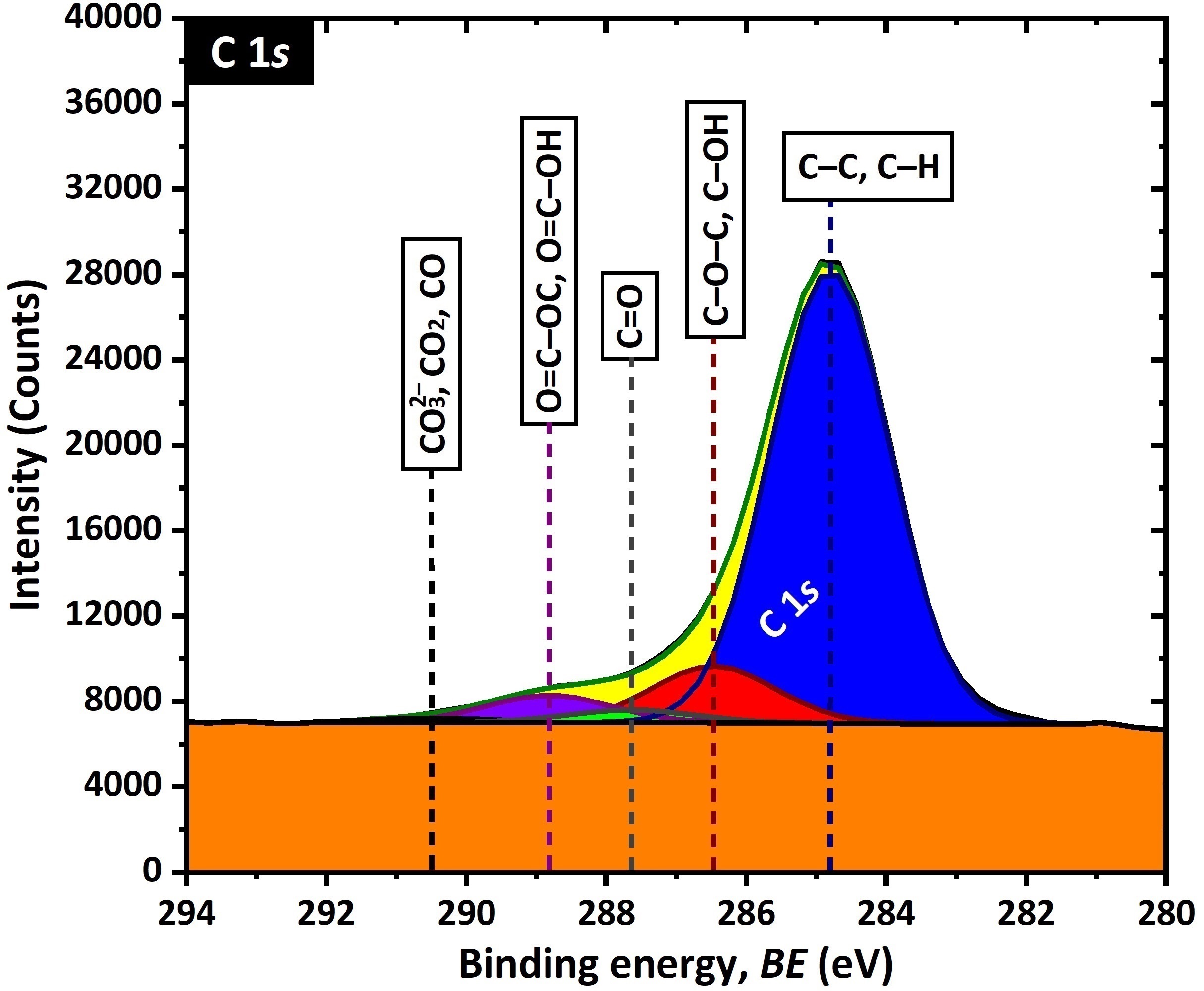
Figure 2 shows the resolved photoelectron spectrum of the C 1s core level for the CdSe thin film deposited for 5 h, which is essential for a proper binding energy correction. In this way, the C 1s component associated to carbon involved in the C–C and C–H bonding is fixed at 284.80 eV. The energy positions and FWHM values employed for the other C 1s components in the C 1s peak fitting are presented in Table 2.

XPS spectrum of the CdSe chemically deposited during 5 h of reaction for the C 1s core level energy region.
Binding energy positions and FWHM values employed in the C 1s peak fitting for each component of the C 1s photoelectron signal according to the carbon chemical environment. The component associated to carbon in the C–C and C–H bonding was fixed at 284.80 eV.
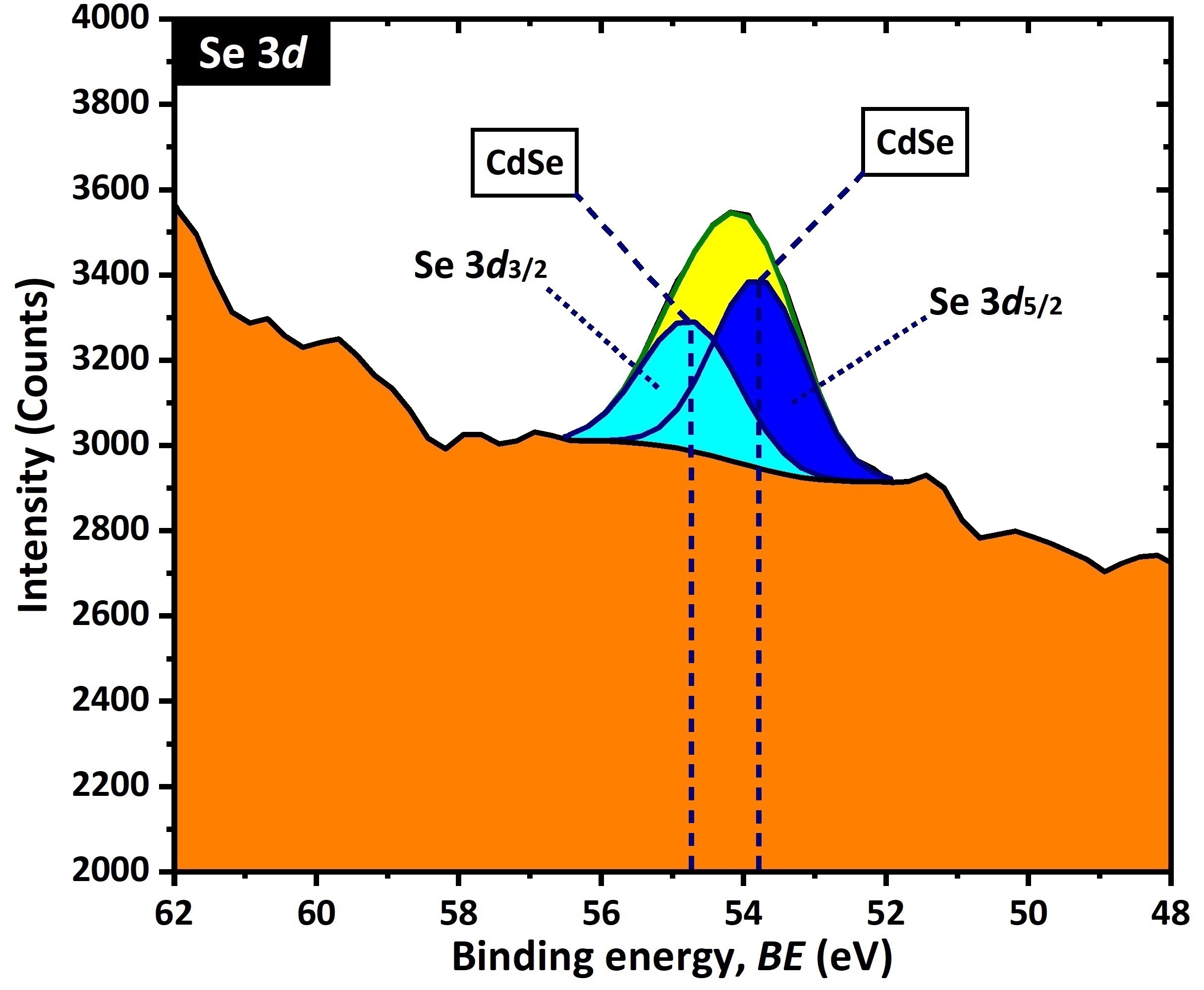
To corroborate that the elements cadmium and selenium detected in the photoelectron spectrum are forming CdSe, the Cd 3d5/2 and Se 3d5/2 signals are usually analyzed. The reason for this is that such signals have been considered the most useful photoelectron lines for the identification of chemical states of the elements cadmium and selenium, as is noticed in the handbook compiled by Moulder et al.25 In this regard, Figure 3 shows the resolved XPS spectrum for the Cd 3d core level, whereas Figure 4 shows the resolved spectrum for the Se 3d core level. With this analysis, the energy position of the Cd 3d5/2 and Cd 3d3/2 peaks were easily identified at 405.31 and 412.06 eV, respectively, showing a spin-orbit splitting of 6.75 eV and a d5/2:d3/2 peak area ratio of 2.97:2 (equal to 1.49); these results agree with the data compiled by Moulder et al.25 for CdSe material. Components associated to oxide species were also found as part of the Cd 3d signals. The energy positions and FWHM values employed for all the components during the peak fitting of the Cd 3d core level are summarized in Table 3.

XPS spectrum of the CdSe chemically deposited during 5 h of reaction for the Cd 3d core level energy region.

XPS spectrum of the CdSe chemically deposited during 5 h of reaction for the Se 3d core level energy region.
Binding energy positions and FWHM values employed in the Cd 3d peak fitting for each component of the Cd 3d photoelectron signals according to the cadmium chemical environment. The photoelectron spectrum was corrected by fixing the C 1s main component at 284.80 eV.
On the other hand, the Se 3d photoelectron signal (Figure 4), which at first sight appears to be a single peak with a maximum at about 54.15 eV, was deconvolved in the Se 3d5/2 and Se 3d3/2 components, identified at 53.78 and 54.74 eV, respectively, showing a spin-orbit splitting of 0.96 eV and a d5/2:d3/2 peak area ratio of 2.77:2 (equal to 1.39). The binding energy value for Se 3d5/2 lies in the energy range of data compiled by Moulder et al.25 for selenides. The energy positions and FWHM values employed for the two mentioned components during the peak fitting of the Se 3d core level are summarized in Table 4. This is the first time that a proper deconvolution analysis is performed for XPS data of CdSe obtained by chemical solution deposition, in terms of correct processing and interpretation of XPS data; for this reason, the identified values for Cd 3d and Se 3d core levels serve as reference for other works dealing on CdSe material.
Binding energy positions and FWHM values employed in the Se 3d peak fitting for each component of the Se 3d photoelectron signal according to the selenium chemical environment. The photoelectron spectrum was corrected by fixing the C 1s main component at 284.80 eV.
Furthermore, it is noteworthy that the detection of sulfur in the sample, through the S 2p signal found at about 167.9 eV (not deconvolved), in a position where the very weak Se 3p1/2 signal is overlapped, as well as the S 2s centered at 231.4 eV, indicates the likely presence of a sulfur-containing compound as a contaminant on the CdSe thin film surface. Although this is the first time in which the presence of sulfur in the CdSe films is detected by means of the XPS technique, this observation has been previously mentioned by some authors26-29. Among them, Hodes et al.26 reported that this small but persistent amount of sulfur in the chemically deposited CdSe layers comes from the Na2SeSO3 reagent. In an almost similar suggestion, Ndiaye & Youm28 reported that this small amount of sulfur, detected by means of energy-dispersive X-ray spectroscopy (EDXS), comes from SO32– ions adsorption. On the other hand, Němec et al.29 found that the amount of sulfur, detected by using the electron microprobe (EMP) analysis, increased with the increase in the concentration of cadmium sulfate (CdSO4) in the reaction solution when this reagent is used as the cadmium source, and suggested the likely formation of cadmium–sulfate complexes or cadmium–sulfate–hydroxo complexes on the surface of the film.
By considering the above, the sulfur detected by XPS in the present work could be bonded to oxygen atoms forming sulfites or sulfates rather than being present as a sulfide. In fact, the position of the detected S 2p signal lies in the energy position range of the S 2p3/2 photoelectron line reported by Moulder et al.25 for such sulfur species, and not in the sulfide range—in fact, there is no S2– ion source in the used aqueous system. This observation agrees with the results of Němec et al.29, who discarded the formation of CdS or CdSxSe1–x in the CdSe films. Thus, taking into account the reagents used in the present work, the most probable residual sulfur species found in the CdSe film surface could be SeSO32– and, mainly, SO32–. On the other hand, we believe that the predominance of the selenium XPS signals over the sulfur ones, and even over the glass component signals, is possible by favoring the deposition of more CdSe material, which is possible by increasing the reaction time or the concentration of Na2SeSO3 in the reaction solution.
Regarding the surface morphology, Figure 5 shows the AFM images of the CdSe thin films deposited during the three different reaction times studied: 5, 7, and 9 h. This figure, in which the height scale is different for a better appreciation, shows that the samples studied are constituted mainly by two types of morphological structures. The first and most fundamental structure is a base-layer formed by the coalescence of CdSe primary particles, which, for the three cases studied, showed sizes of about 100 nm. The second structure, which is actually a late-structure that grows on the surface of this base-layer, seems to be composed of large aggregates of many secondary particles that probably form cauliflower-like clusters that appear in the AFM images in the form of mountain-like protruding structures. These protruding structures are strongly adhered to the film surface, as they remained attached to the surface even after the cleaning treatment with the wet cotton ball applied immediately after obtaining the CdSe films. As presented in Table 5, the sizes of these mountain-like structures (as they will be referred to in this paper) increased with the increase of reaction time, from about 0.5 μm at 5 h to about 0.9 μm at 9 h of reaction. Meanwhile, as also presented in Table 5, the increase in the reaction time from 5 to 9 h does not significantly influence the size of the base-layer particles, although a slight increase is observed.

AFM images of CdSe thin films chemically deposited during (a) 5, (b) 7, and (c) 9 h of reaction.
Base-layer particle size and mountain-like structure size of the CdSe thin films deposited during different reaction times.
When comparing the surface morphological structures observed in this work with the surface images of CdSe reported in the scientific literature, a greater similarity was found with the AFM and SEM images presented by Agrawal et al.11, where a granular film with some protruding aggregates of a few particles is observed. There is also some similarity with the CdSe film deposited at 50 °C and 15 min reported in the work of Sanchez-Ramirez et al.12, which consists of a granular film with rough, granular, and almost spherical clusters over its surface, but our results are completely different when compared to the films deposited at 75 and 90 °C, which show a morphological tendency from the nearly spherical clusters with rough, granular surface texture (bitter orange-like morphology) to clusters composed of several nanosheets or flakes that are interconnected which each other (flower-like morphology). In fact, although other authors have observed a granular film with some or various simple aggregates on its surface (with a structure ranging from a few particles to a cauliflower-like morphology)30-37, surface images showing protruding clusters with complex morphologies are also found in the CdSe scientific literature12,28,38-43. It is important to note that there is still no published work that explains the conditions that lead to one or the other morphology, although there is evidence that the obtained morphology is probably related to synthesis conditions such as reaction temperature12,41 and initial pH42, and also to the annealing temperature28,33,38,39 and even the color of the light that irradiates the reaction43. This makes it clear that a systematic work on the effect of the conditions mentioned above would be very interesting for future research. This future study should employ a high-resolution SEM to adequately detect the subtle details of the substructure of each grain and cluster, as we believe that some of the grains and clusters shown in the SEM images of the apparently simple granular films reported in the scientific literature actually exhibit a complex flower-like morphology (interconnected flakes or needles)36,37, similar to the SEM images presented by Ndiaye & Youm28; however, it was the low microscope resolution used in the aforementioned works that did not allow these details of the substructure to be detected.
Finally, but no less importantly, Figure 6 shows the variation of the roughness of the three CdSe thin films as a function of the reaction time. This graph clearly shows that the roughness increased with the increase of reaction time. With the latter, it is concluded that the values of the main surface parameters of the chemically deposited CdSe thin films increase as reaction time increases.

Variation of the roughness of the chemical-solution-deposited CdSe films as a function of the reaction time.
4. Conclusions
The CdSe thin films that were obtained by chemical solution deposition from a CdCl2–N(CH2CH2OH)3–NH3–Na2SeSO3–Na2SO3 aqueous system showed a n-type conductivity and a sulfur content on their surface. This presence of sulfur, associated to residual SO32– and SeSO32– species over the CdSe thin film, can be detected by a simple XPS analysis. This XPS analysis also corroborates that the deposited material is indeed CdSe, with energy positions of Cd 3d5/2 and Se 3d5/2 located at 405.31 and 53.78 eV, respectively. Apparently, the thin films are constituted by a layer of primary particles, as a base structure, and by aggregates of secondary particles forming mountain-like structures (probably clusters with cauliflower-like morphology), as a late-structure that grows over the base-layer and which becomes more predominant as the reaction time is longer. As a final conclusion, the values of the base-layer particle size, mountain-like structure size, and roughness definitely increase with the increase of the reaction time.
5. Acknowledgments
The authors are grateful to R. Mora-Monroy for the technical assistance in the XPS measurements. Special thanks go to M. Sotelo-Lerma for her unconditional help that was essential to complete the present research.
6. Data Availability
Data that support the findings of this study will be made available upon reasonable request to the corresponding author.
7. References
-
1 Chopra KL, Kainthla RC, Pandya DK, Thakoor AP. Chemical solution deposition of inorganic films. In: Hass G, Francombe MH, Vossen JL, editors. Physics of thin films: advances in research and development. New York: Academic Press; 1982. p. 167-235. (vol. 12). https://doi.org/10.1016/S0079-1970(13)70010-0
» https://doi.org/10.1016/S0079-1970(13)70010-0 - 2 Hodes G, Fonash SJ, Heller A, Miller B. Photoelectrochemical cells based on polycrystalline semiconductors. In: Gerischer H, editor. Advances in electrochemistry and electrochemical engineering. New York: John Wiley & Sons; 1984. p. 113-58. (vol. 13).
-
3 Lokhande CD. Chemical deposition of metal chalcogenide thin films. Mater Chem Phys. 1991;27(1):1-43. https://doi.org/10.1016/0254-0584(91)90158-Q
» https://doi.org/10.1016/0254-0584(91)90158-Q -
4 Nair PK, Nair MTS, García VM, Arenas OL, Peña Y, Castillo A, et al. Semiconductor thin films by chemical bath deposition for solar energy related applications. Sol Energy Mater Sol Cells. 1998;52(3-4):313-44. https://doi.org/10.1016/S0927-0248(97)00237-7
» https://doi.org/10.1016/S0927-0248(97)00237-7 -
5 Savadogo O. Chemically and electrochemically deposited thin films for solar energy materials. Sol Energy Mater Sol Cells. 1998;52(3-4):361-88. https://doi.org/10.1016/S0927-0248(97)00247-X
» https://doi.org/10.1016/S0927-0248(97)00247-X -
6 Lincot D, Froment M, Cachet H. Chemical deposition of chalcogenide thin films from solution. In: Alkire RC, Kolb DM, editors. Advances in electrochemical science and engineering. Weinheim: Wiley-VCH Verlag GmbH; 1999. p. 165-235. (vol. 6). https://doi.org/10.1002/9783527616800.ch3
» https://doi.org/10.1002/9783527616800.ch3 -
7 Mane RS, Lokhande CD. Chemical deposition method for metal chalcogenide thin films. Mater Chem Phys. 2000;65(1):1-31. https://doi.org/10.1016/S0254-0584(00)00217-0
» https://doi.org/10.1016/S0254-0584(00)00217-0 -
8 Hodes G. Chemical solution deposition of semiconductor films [Internet]. New York: Marcel Dekker; 2003 [cited 2026 Jan 13]. Chapters 2, 4 and 9. Available from: https://books.google.es/books?id=PjmQnVX4OmUC&printsec=frontcover&source=gbs_ge_summary_r&cad=0#v=onepage&q&f=false
» https://books.google.es/books?id=PjmQnVX4OmUC&printsec=frontcover&source=gbs_ge_summary_r&cad=0#v=onepage&q&f=false -
9 Sengupta S, Aggarwal R, Raula M. A review on chemical bath deposition of metal chalcogenide thin films for heterojunction solar cells. J Mater Res. 2023;38(1):142-53. https://doi.org/10.1557/s43578-022-00539-9
» https://doi.org/10.1557/s43578-022-00539-9 -
10 Rai BK, Bist HD, Katiyar RS, Nair MTS, Nair PK, Mannivannan A. Simultaneous observation of strong and weak quantum confinement effect in chemically deposited CdSe thin films: a spectro-structural study. J Appl Phys. 1997;82(3):1310-9. https://doi.org/10.1063/1.365904
» https://doi.org/10.1063/1.365904 -
11 Agrawal P, Sachdeva M, Singh A, Bhargava A. Effect of deposition temperature and time on the structural, optical and morphological properties of nanocrystalline CdSe thin films deposited by chemical bath deposition. Int J Educ Appl Res [Internet]. 2014 [cited 2026 Jan 13];4(2, Suppl 1):22-5. Available from: https://www.researchgate.net/publication/265551553
» https://www.researchgate.net/publication/265551553 -
12 Sanchez-Ramirez EA, Hernandez-Perez MA, Aguilar-Hernandez JR, Palacios-Beas EG, Villanueva-Ibañez M. Temperature and deposition time effect on properties and kinetics of CdSe and CdS0.25Se0.75 films deposited by CBD. Mater Res. 2017;20(4):1121-8. https://doi.org/10.1590/1980-5373-mr-2016-0728
» https://doi.org/10.1590/1980-5373-mr-2016-0728 -
13 Pawar SA, Patil DS, Shin JC. Cadmium selenide microspheres as an electrochemical supercapacitor. Mater Today Chem. 2017;4:164-71. https://doi.org/10.1016/j.mtchem.2017.04.002
» https://doi.org/10.1016/j.mtchem.2017.04.002 -
14 Mondal A, Chaudhuri TK, Pramanik P. Deposition of cadmium chalcogenide thin films by a solution growth technique using triethanolamine as a complexing agent. Sol Energy Mater. 1983;7(4):431-8. https://doi.org/10.1016/0165-1633(83)90016-3
» https://doi.org/10.1016/0165-1633(83)90016-3 - 15 Fofanov GM, Kitaev GA. Analysis of the conditions for the precipitation of metal selenides from aqueous solutions with sodium selenosulphate. Russ J Inorg Chem. 1969;14(3):322-4.
- 16 Kitaev GA, Terekhova TS. Analysis of the conditions for the precipitation of cadmium selenide from aqueous sodium selenosulphate solutions. Russ J Inorg Chem. 1970;15(1):25-7.
-
17 García-Valenzuela JA, Castelo-González OA, Baez-Gaxiola MR, Sotelo-Lerma M. Detailed analysis of five aspects addressed to minimize costs and waste in the chemical bath deposition of CdS films using the CdB–AC6H5O7–AOH–(NH2)2CS System. Mater Sci Appl. 2013;4(6):386-405. https://doi.org/10.4236/msa.2013.46049
» https://doi.org/10.4236/msa.2013.46049 -
18 García-Valenzuela JA, Cota-Leal M, Corona-Martínez DO, Baez-Gaxiola MR, Martínez-Gil M, Sotelo-Lerma M, et al. On the adherence of chemically deposited CdS films to common inorganic substrates: effect of Cd2+ concentration in solution, substrate surface chemistry, and reaction temperature. ChemistrySelect. 2019;4(5):1650-65. https://doi.org/10.1002/slct.201803033
» https://doi.org/10.1002/slct.201803033 -
19 Cota-Leal M, García-Valenzuela JA. Chemical solution deposition of Al(OH)3-AlOOH films: application for surface sensitizing of rigid and flexible substrates to improve the adhesion in coating technology areas. ChemistrySelect. 2021;6(24):6083-96. https://doi.org/10.1002/slct.202101449
» https://doi.org/10.1002/slct.202101449 -
20 García-Valenzuela JA, Baez-Gaxiola MR, Cota-Leal M. Problems with the adhesion of chemical-solution-deposited films? Solving the problem of CdS thin film adhesion with a very simple and green chemical procedure. Chem Lett. 2022;51(2):177-81. https://doi.org/10.1246/cl.210667
» https://doi.org/10.1246/cl.210667 -
21 Rosas-Domínguez CJ, Escalante-Bujanda MA, Sandoval-Sánchez RI, Vargas-Durazo JT, Corona-Martínez DO, García-Valenzuela JA. Efecto de la concentración del ligante citrato (C6H5O73–) en la adherencia de películas de CdS obtenidas por depósito en solución química sobre sustratos de vidrio utilizando el sistema CdCl2–Na3C6H5O7–NaOH–SC(NH2)2 J BioProcess Chem Technol [Internet]. 2026 [cited 2026 Jan 13];18(36):30-40. Available from: https://revistas.uadec.mx/index.php/JBCT/article/view/796
» https://revistas.uadec.mx/index.php/JBCT/article/view/796 -
22 García-Valenzuela JA, Baez-Gaxiola MR, Sotelo-Lerma M. Chemical bath deposition of PbS thin films on float glass substrates using a Pb(CH3COO)2–NaOH–(NH2)2CS–N(CH2CH2OH)3–CH3CH2OH definite aqueous system and their structural, optical, and electrical/photoelectrical characterization. Thin Solid Films. 2013;534:126-31. https://doi.org/10.1016/j.tsf.2013.02.035
» https://doi.org/10.1016/j.tsf.2013.02.035 -
23 Cabrera-German D, García-Valenzuela JA, Cota-Leal M, Martínez-Gil M, Aceves R, Sotelo-Lerma M. Detailed characterization of good-quality SnS thin films obtained by chemical solution deposition at different reaction temperatures. Mater Sci Semicond Process. 2019;89:131-42. https://doi.org/10.1016/j.mssp.2018.09.009
» https://doi.org/10.1016/j.mssp.2018.09.009 -
24 Cota-Leal M, García-Valenzuela JA, Cabrera-German D, Martínez-Gil M, Paredes-Sotelo E, Sotelo-Lerma M. Synthesis of CH3NH3PbI3–xClx perovskite by the three-step route consisting of chemical solution deposition followed by gas–solid reaction transformations: film quality and photodetector performance evaluation. Org Electron. 2019;73:76-86. https://doi.org/10.1016/j.orgel.2019.05.049
» https://doi.org/10.1016/j.orgel.2019.05.049 - 25 Moulder JF, Stickle WF, Sobol PE, Bomben KD. Handbook of X-ray photoelectron spectroscopy: a reference book of standard spectra for identification and interpretation of XPS data. Eden Prairie: Physical Electronics; 1995.
-
26 Hodes G, Albu-Yaron A, Decker F, Motisuke P. Three-dimensional quantum-size effect in chemically deposited cadmium selenide films. Phys Rev B Condens Matter. 1987;36(8):4215-21. https://doi.org/10.1103/PhysRevB.36.4215
» https://doi.org/10.1103/PhysRevB.36.4215 -
27 Cerdeira F, Torriani I, Motisuke P, Lemos V, Decker F. Optical and structural properties of polycrystalline CdSe deposited on titanium substrates. Appl Phys, A Solids Surf. 1988;46(2):107-12. https://doi.org/10.1007/BF00615917
» https://doi.org/10.1007/BF00615917 -
28 Ndiaye A, Youm I. Effects of post-deposition processing on microstructural properties of cadmium selenide thin films grown from solution. Eur Phys J Appl Phys. 2003;23(2):75-82. https://doi.org/10.1051/epjap:2003047
» https://doi.org/10.1051/epjap:2003047 -
29 Němec P, Šimurda M, Němec I, Sprinzl D, Formánek P, Malý P. Highly luminescent CdSe nanocrystalline films prepared by chemical bath deposition. J Cryst Growth. 2006;292(1):78-86. https://doi.org/10.1016/j.jcrysgro.2006.03.057
» https://doi.org/10.1016/j.jcrysgro.2006.03.057 -
30 Boudreau RA, Rauh RD. Chemical bath deposition of thin film cadmium selenide for photoelectrochemical cells. J Electrochem Soc. 1983;130(2):513-6. https://doi.org/10.1149/1.2119741
» https://doi.org/10.1149/1.2119741 -
31 Vargas-Hernández C, Lara VC, Vallejo JE, Jurado JF, Giraldo O. XPS, SEM and XRD investigations of CdSe films prepared by chemical bath deposition. Phys Status Solidi, B Basic Res. 2005;242(9):1897-901. https://doi.org/10.1002/pssb.200461717
» https://doi.org/10.1002/pssb.200461717 -
32 Hernandez-Perez MA, Aguilar-Hernandez J, Contreras-Puente G, Vargas-García JR, Rangel-Salinas E. Comparative optical and structural studies of CdSe films grown by chemical bath deposition and pulsed laser deposition. Physica E. 2008;40(7):2535-9. https://doi.org/10.1016/j.physe.2007.10.102
» https://doi.org/10.1016/j.physe.2007.10.102 -
33 Shyju TS, Anandhi S, Indirajith R, Gopalakrishnan R. Effects of annealing on cadmium selenide nanocrystalline thin films prepared by chemical bath deposition. J Alloys Compd. 2010;506(2):892-7. https://doi.org/10.1016/j.jallcom.2010.07.106
» https://doi.org/10.1016/j.jallcom.2010.07.106 -
34 Khomane AS. Structural and optical characterizations of chemically deposited cadmium selenide thin films. Mater Res Bull. 2011;46(10):1600-3. https://doi.org/10.1016/j.materresbull.2011.06.011
» https://doi.org/10.1016/j.materresbull.2011.06.011 -
35 Deshpande MP, Garg N, Bhatt SV, Sakariya P, Chaki SH. Characterization of CdSe thin films deposited by chemical bath solutions containing triethanolamine. Mater Sci Semicond Process. 2013;16(3):915-22. https://doi.org/10.1016/j.mssp.2013.01.019
» https://doi.org/10.1016/j.mssp.2013.01.019 -
36 Chavan GT, Pawar ST, Prakshale VM, Sikora A, Pawar SM, Chaure NB, et al. Quaternary schematics for property engineering of CdSe thin films. Appl Surf Sci. 2017;426:466-79. https://doi.org/10.1016/j.apsusc.2017.07.208
» https://doi.org/10.1016/j.apsusc.2017.07.208 -
37 Önal M, Altiokka B. A new approach in chemical bath deposition of cadmium selenide thin films. Phys Status Solidi A Appl Mater Sci. 2025;222(2):2400268. https://doi.org/10.1002/pssa.202400268
» https://doi.org/10.1002/pssa.202400268 -
38 Kale RB, Lokhande CD. Systematic study on structural phase behavior of CdSe thin films. J Phys Chem B. 2005;109(43):20288-94. https://doi.org/10.1021/jp053124c
» https://doi.org/10.1021/jp053124c -
39 Pawar SA, Devan RS, Patil DS, Moholkar AV, Gang MG, Ma Y-R, et al. Improved solar cell performance of chemosynthesized cadmium selenide pebbles. Electrochim Acta. 2013;98:244-54. https://doi.org/10.1016/j.electacta.2013.03.016
» https://doi.org/10.1016/j.electacta.2013.03.016 -
40 Chikwenze RA, Nwofe PA, Agbo PE, Nwankwo SN, Ekpe JE, Nweke FU. Effect of dip time on the structural and optical properties of chemically deposited CdSe thin films. Int J Mater Sci Appl. 2015;4(2):101-6. https://doi.org/10.11648/j.ijmsa.20150402.15
» https://doi.org/10.11648/j.ijmsa.20150402.15 -
41 Hatam EG, Ghobadi N. Effect of deposition temperature on structural, optical properties and configuration of CdSe nanocrystalline thin films deposited by chemical bath deposition. Mater Sci Semicond Process. 2016;43:177-81. https://doi.org/10.1016/j.mssp.2015.12.013
» https://doi.org/10.1016/j.mssp.2015.12.013 -
42 Piryaei M, Gholami Hatam E, Ghobadi N. Influence of pH on the optical, structural and compositional properties of nanocrystalline CdSe thin films prepared by chemical bath deposition. J Mater Sci Mater Electron. 2017;28(3):2550-6. https://doi.org/10.1007/s10854-016-5830-5
» https://doi.org/10.1007/s10854-016-5830-5 -
43 Pawar SW, Tabhane VA, Lokhande PE, Khan F, Kaur J, Al-Ahmed A, et al. Structural, morphological and optical characterization of photochemically deposited cadmium selenide thin films. ES Energy & Environment [Internet]. 2022 [cited 2026 Jan 13];17:106-13. Available from: https://www.espublisher.com/journals/articledetails/652/
» https://www.espublisher.com/journals/articledetails/652/