Enhanced Performance of Al/Nb2O5/Pt/Nb2O5/Ag Microwave Resonators Designed as Bandstop Filters and Negative Capacitance Sources
Abstract
Herein stacked layers of Nb2O5 coated onto Al substrates are fabricated as microwave resonators. Structural and morphological analyses on these stacked layers have shown the amorphous nature of growth of the stacked layers. Electrically, the resonators showed negative capacitance effect accompanied with series and parallel resonance at three well -distinguished notch frequencies. Additionally, the resonators exhibited bandstop filter characteristics with notch frequency () centered at 1.05 GHz, return loss () value of 9.0 dB and voltage standing wave ratios () of 2.12. To enhance the performance of the Nb2O5 microwave resonators, platinum nanosheets of thicknesses of 50 nm were inserted between layers of Nb2O5. Platinum nanosheets successfully decreased the surface roughness and increase the electrical conductivity by five orders of magnitude. Pt nanosheets additionally improved the values of , , and to 1.16 GHz, 0.039, 30.3 dB and 1.12, respectively. The features of the microwave resonators comprising Pt nanosheets in its structure are promising for using them in communication technology.
Keywords:
Nb2O5/Pt/Nb2O5; Microwave resonators; Return loss; Gigahertz; Negative capacitance
1. Introduction
Niobium pentoxide is one of the oxide materials that have recently captured attention due to its important role in electronics. This material has successfully improved the performance of multi-qubit superconducting processors1. These processors experienced microwave loss, which was reduced by the fabrication of niobium pentoxide-based superconducting circuits under a high vacuum pressure1. Nb2O5 is also employed for the fabrication of three-dimensional superconducting resonators. The superconducting resonators have shown three resonant frequencies centered at 1.30, 2.60, and 5.0 GHz operating at 10 mK2. This feature of the resonators allowed for extending the photon lifetime up to 2.0 seconds2. In addition, due to the high thermodynamic stability of the niobium–oxygen system, Nb2O5 fabricated by the electron beam technique was used as a low-loss coplanar waveguide resonator3. For a coplanar resonator with a gap of 2.0 μm, a loss tangent of 1.5×10⁻⁷ was achieved in the single-photon regime3. Moreover, Nb2O5 has been used in thin film transistor technology, functioning as resistive memory devices4. These devices were fabricated with two different electrodes made of Au and Cu as top and bottom electrodes, respectively. The device displayed resistive switching performance with an “on/off” ratio of 105 at an ultra-low operating voltage down to 2 mV4.
Because of the smart features of electronic devices achieved by using niobium pentoxide, in this work, we are motivated to fabricate a new class of microwave resonators to perform as bandstop filters suitable for communication technology. The resonators are made of two stacked layers of Nb2O5 deposited onto aluminum thin film substrates serving as bottom electrodes and top-contacted with a silver point contact. Aluminum is selected as a substrate to deposit Nb2O5 because of the strong interaction between these two layers, forming Al2O3-Nb2O5 interacting regions at the nanoscale level5. These interfaced layers are employed as tunnel rectifiers suitable for infrared energy harvesting6.
This structure has shown rectification performance adequate for inclusion in rectenna arrays. These arrays are used for infrared energy harvesting, showing a current responsivity of 4.3 A/W at 0.35 V6. The novelty of the current work lies in fabricating microwave resonators that operate at room temperature and exhibit bandstop filter characteristics in addition to the series-parallel resonance switching property. Another novelty of the current work lies in enhancing the performance of the niobium pentoxide microwave resonators through the insertion of Pt nanosheets between the stacked layers of Nb2O5. The work will provide information about the notch frequencies, the magnitude of the reflection coefficient, the return loss values, and the voltage standing wave ratios of the resonators.
2. Experimental Details
The fabrication of the Al/Nb2O5/Pt/Nb2O5/Ag microwave resonators was initiated by depositing a thin film of aluminum with a thickness of 1.0 μm onto ultrasonically cleaned glass substrates using the thermal evaporation technique under a vacuum pressure of 10-5 mbar. Next, stacked layers of Nb2O5 with thicknesses of 350 nm (each layer) were coated onto the Al substrates. These layers were deposited using SPT-2 type sputtering machine using high purity (99.95%, Alfa Aeser) Nb2O5 sputtering target. The ion coating technique is preferred here because it allow for producing Nb2O5 in a relatively shorter period of time compared to the thermal evaporation technique. For some of the samples, the coating process started by depositing the first Nb2O5 first layer and then coating this layer with platinum nanosheets of thicknesses of 50 nm before stacking with the second layer. In this part of experiment, a high purity (99.99%, Alfa Aeser) Pt sputtering target was used. The top Nb2O5 layer was coated with high purity (99.9%) point contact Ag paste. The structural and morphological analyses were conducted with the help of a Miniflex- 600 X-ray diffraction unit and a scanning electron microscope (COXEM-200). The roughness and thickness of the films were investigated using a SOLID IN II profilometer. The conductivity type was determined using the standard hot probe technique. The room temperature electrical conductivity of the Hall bar shaped samples was measured with the help of an automated Keithley –IV-system. The impedance spectra were recorded using an Agilent 4291B impedance analyzer.
3. Results and Discussion
In this work, we focus on the design and characterization of a new class of microwave resonators (bandstop filters) made of niobium pentoxide thin layers. The geometrical design of the bandstop filters is shown as an inset in Figure 1a. The study here includes two types of filters: one is composed of two stacked layers of Nb2O5 grown onto Al substrates (abbreviated as ANPN-00) and the other is composed of two stacked layers of Nb2O5 sandwiched with platinum nanosheets with thicknesses of 50 nm (abbreviated as ANPN-50). The X-ray diffraction patterns collected from these two devices reveal no sharp peaks except for those centered at diffraction angles of 2θ = 38.8° which are well known as the maximum reflection of face-centered cubic aluminum along the (111) plane direction (PDF card number 01-089-2837). In accordance with the XRD patterns, the grown stacked layers of Nb2O5 exhibit an amorphous nature of structure. The amorphous nature of growth is also confirmed by the scanning electron microscopy (SEM) technique. SEM images shown in Figure 1b and 1c for ANPN-00 and ANPN-50, respectively, display no grains even at magnifications of 30000-40000 of the tested surface. The films are amorphous because they were deposited at low temperature7. Amorphous niobium pentoxide is reported to be preferable for use as electrodes in supercapacitors to store energy8. As also seen from Figure 1a and 1c, the insertion of Pt nanosheets between stacked layers of niobium pentoxide did not alter the structural properties and surface morphology of the films.

(a) The X-ray diffraction patterns and the scanning electron microscopy images for (b) ANPN-00 and (c) ANPN-50 films. Inset of (a) showing the geometrical design of the device under study.
The absence of grains from the films indicates that the surface is homogeneous9. Such a phenomenon was previously observed by Mo doping into Ti(C, N)-based materials9. Smaller grains actually lead to smaller surface rugosity and less roughness10. This expectation is confirmed by measuring the roughness parameters for the devices before and after the insertion of Pt nanosheets. The average () and mean root square roughness () value of ANPN-00 devices decreased from =21 nm = 21 and =41 nm to =13 nm and ()=38 nm, respectively, after the insertion of Pt nanosheets. Lower roughness values are reported to result from modification of the film morphology by doping10. Lower roughness values achieved by doping also result in higher electrical conductivity values11,12. Experimentally, we observed that stacked layers of Nb2O5 coated onto glass substrates (non-conducting media of poor thermal conductivity) exhibited p-type conductivity with room temperature conductivity values of 7.4×10⁻⁷(Ωcm)−1. The conductivity remarkably increased to 1.8×10⁻¹(Ωcm)−1 and was converted to n-type after the insertion of Pt layers with a thickness of 50 nm. The conductivity increased by five orders of magnitude. These achievements, which resulted in a smoother surface and enhanced electrical conductivity, can be ascribed to the ionic substitution of Pt+4 in vacant sites of Nb5+. The p-type conductivity usually results from the availability of excess anions (excess oxygen) in Nb2O5. The n-type conductivity indicates the existence of excess cations in the compound. Since the ionic radius of Nb+5 is 64 pm13 and is larger than that of Pt4+ (62.5 pm14), Pt4+ ions can be substituted in vacant sites of Nb. The bond length of Nb-O in Nb2O5 is 213 pm15, which is larger than that of Pt-O, reported as 202-206 pm16. Thus, the shorter bond lengths of Pt-O compared to Nb-O cause a stronger covalent structure and a more stable system17. The stability of the structure is also accompanied by a higher degree of orbital overlapping between the orbital states of Pt (4f145d96s1) and Nb2O5 because they are at higher orbital energies compared to Nb (5s24d4)18. Strong orbital overlapping results in the formation of orbital states close to the conduction band edge, thereby increasing the electrical conductivity of the materials. Such phenomena were previously observed in Pb/FeSe2 interface devices19.
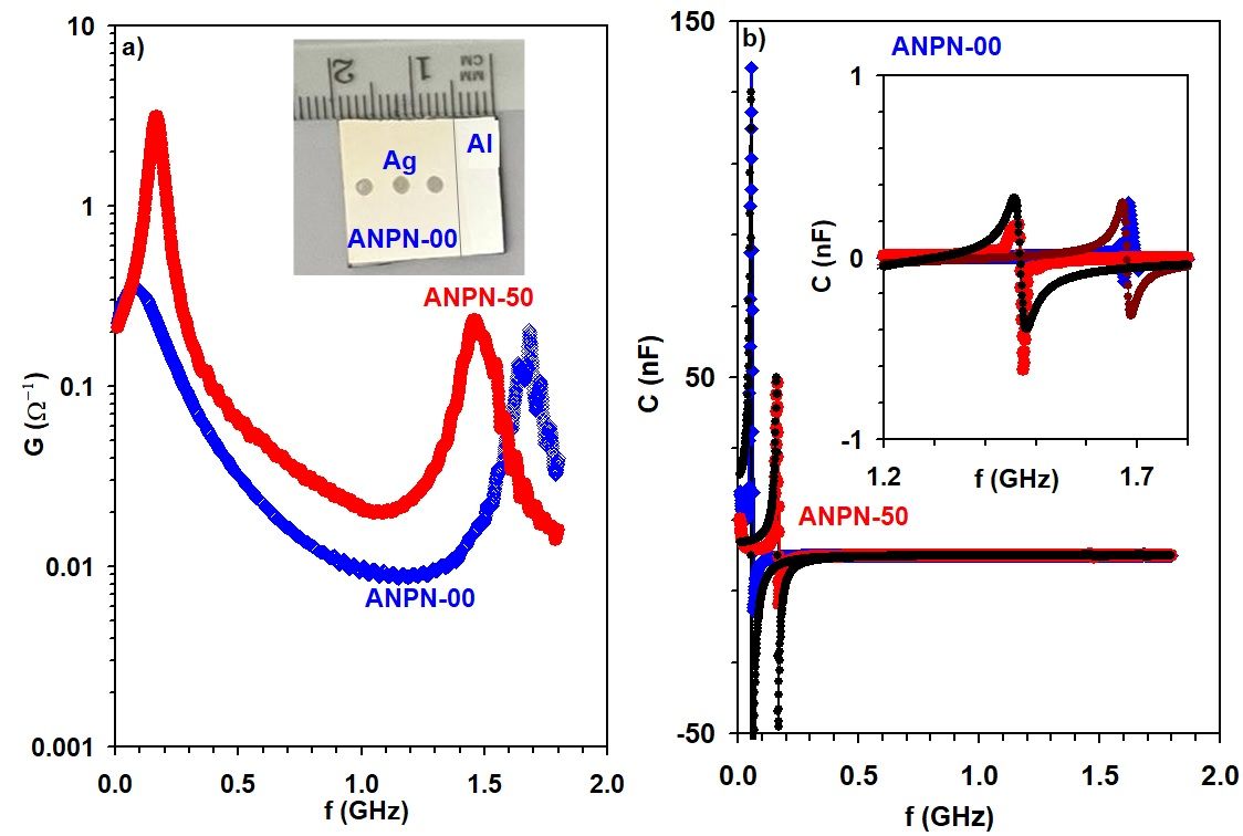
The features of the ANPN-50 device structure presented by lower roughness and enhanced electrical conductivity achieved by insertion of Pt nanosheets make the device structure promising for use in microwave technology19,20. As a confirming tool, the device was top contacted with Ag point contact. The optical image of the device comprising three contact points is shown in the inset of Figure 2a. Keeping in mind that Pt nanosheets are not in contact with outer side of Nb2O5, Ag contact is preferred to establish a different built- in potential () at the Ag/Nb2O5 interface compared to that of Al/Nb2O5. The difference between the potential barriers of Ag (eV) and Al (21) is eV. Different built in potentials cause the formation of an internal electric field that in turn leads to asymmetric electrical characteristics in hybrid structured devices22. This method is also known for the formation of microwave resonators that exhibit more than one resonance frequency23. It was shown that second harmonic microwave generation can be achieved with different built-in potentials of diodes23. In addition, due to the different built-in potential values, anti-domain structures performing as nanocapacitors are formed. These capacitors exhibit different resonance frequencies based on their internal dielectric responses24. For our case the strong interaction between Al and Nb2O5 leads to the formation of Al2O3-Nb2O5 nano- dielectric layers (capacitors) which satisfy these additional conditions5.

(a) The conductance and (b) the capacitance spectra for ANPN-xx microwave band filters. The inset of (a) showing the optical image of the sample. The inset of (b) showing the high capacitance series and parallel resonance in the high frequency domain.
The ANPN-xx device fabricated here are connected between the terminals of an impedance analyzer, the measured conductance () and capacitance () spectra are shown in Figure 2a and 2b, respectively. The ac signal amplitude was kept at a minimum and the frequency was varied in the range of 0.01-1.8 GHz. It is clear from Figure 2a that the conductance of ANPN-00 devices shows one broaden and one sharp maxima centered at critical frequency values of 0.075 GHz and 1.685 GHz, respectively. As seen from Figure 2b and its inset the devices exhibit “resonance- antiresonance” capacitive mode at 0.055 GHz and at 1.685 GHz. The insertion of Pt nanosheets increased the conductance value and enhanced the resonance peaks. A shift in the peaks positions from 0.075 to 0.172 GHz and from 1.685 GHz to 1.483 GHz is observed upon insertion of Pt nanosheets (ANPN-50) devices. The resonant peaks observed in the capacitance spectra are also shifted to 0.162 GHz and to 1.467 GHz. The amplitude of the peaks also increased. When the device is in the anti-resonance mode the capacitance go negative. Negative capacitance (NC) effect is also a desirable feature of electronic devices as they cancel out parasitic effects and reduce noise from signals25 It can also serve as signal amplifiers21,25. NC effect appears when there is an imbalance between the amount of polarization switching and the amount of charge supplied to compensate for25.Variations in the NC value and in the position of the resonance peaks can be explained by analyses of the dielectric (=; distance between electrodes (film thickness) and is the area of the electrode) dispersion using Lorentz approach26. The dielectric constant dispersion relation provides information about the free carrier concentration () in the active dielectric region. The dielectric dispersion in accordance with this model are given by the relation26,
Here is the dielectric oscillator frequency, is electronic friction coefficient and is equal to the inverse of the relaxation time constant (). is the reduced effective mass of electrons and/or holes in the oscillatory system. is the high frequency dielectric constant and represent the number of possible oscillators with frequencies The series in Equation 1 represent the dynamical part of capacitance or dielectric spectra. In accordance with the equation, NC effect will dominate under conditions which make this part negative and larger than It is clear from the equation that values of radial frequency () larger than will be the main factor for negative values of dynamical part. The value itself will depend on the damping coefficient or electronic damping coefficient (). The good fitting of Equation 1 to the experimental data is shown by black colored circles in Figure 2b. It is achieved by the parameters shown in Table 1. The calculations shown in Table 1 are obtained by substituting the reduced effective mass of the ANPN-xx system as
Here 27 is the hole effective mass of the type Nb2O5, = and are the electron effective masses of the Pt and Al thin films, respectively. Aluminum is included because it represents the substrate of the oxide layer and is probably reacted with the Nb2O5 layer as previously predicted. The tabulated data provide information about the existence of three notch frequencies () of values of 0.057 GHz, 1.05 GHz and 1.68 GHz. The most significant one is the one displaying highest “resonance-antiresonance” peak which is centered near 0.057 GHz. For this peak the free carrier concentration is the highest and the electronic friction coefficient (=(200 ns)-1) is the least meaning an efficient free carrier oscillation between resonance (series resonance) and antiresonance (parallel resonance) operation modes28. Basically series resonance dominates when the capacitive reactance is equal to the inductive reactance but opposite in phase. Cancelation of these reactances leads to a purely resistive mode of operation with resistive impedance (). In this mode of operation a maximum current flows in the device because the impedance is minimum. Such mode of operation is used for tuning circuits and frequency filters. In contrast to this mode of operation parallel resonance is associated with maximum impedance and minimum current flow. This condition of operation is used in applications such as bandstop filters and impedance matching networks28,29.
It is clear from Table 1 that insertion of Pt nanosheets between layers of Nb2O5 has shifted the notch frequency values (0.057 GHz and 1.05 GHz) to a higher microwave frequency values (0.165 GHz and 1.13 GHz) and decreased both of the relaxation time constants and free carrier concentration. The notch frequency centered at 1.68 GHz is shifted to a lower value of 1.47 GHz. While the scattering time constant decreased, the free carrier concentration associated with this resonance mode increased. For the series resonance mode, the decrease in the time constant means an increase in the damping coefficient or electronic friction. Electronic friction is referred to the dissipation of energy due to the resistance. As the resistance convert lost energy to heat the amplitude of oscillation decreases. This is also clear from the maximum values of the resonance peaks shown in Figure 2b. As for examples the peak centered at 0.057 GHz exhibited an amplitude of 136 nF and decreased to 50 nF (at 0.165 GHz) after insertion of Pt nanosheets. On the other hand damping in parallel resonance causes a decrease in the peak amplitude and a widening of the resonance bandwidth28,30.
Figure 3a illustrates the impedance spectra being calculated from the measured capacitance and conductance spectra ( ; is inductance of the devices)28. The impedance of ANPN-00 microwave resonators increases with increasing signal frequency, displaying a maximum of 108 at 1.05 GHz. It then decreases with increasing signal frequency. Insertion of Pt nanosheets shifted the maximum peak to 1.16 GHz and decreased the impedance value to 46 . This value is very close to the ideal impedance value (50 ) of signal generators. The value of Z being 46 matches the impedance of the feed. Such property solves the problem in feeding and extracting signals efficiently31. Impedance matched band filters are very necessary electronic components used in broadband power- line communications as they play vital role in noise reduction32.

(a) The impedance and (b) the magnitude of the reflection coefficient spectra for Al/Nb2O5/Pt/Nb2O5/Ag microwave resonators.
Practically band filters are defined by their reflection coefficient spectra which are known as parameter. parameter is calculated from the relation between the impedance of the load (ANPN-xx) and the source () using the equation, 28. values of 1.0 and 0.0 means total rejection or transmission of ac signals through the device28. The data of spectra are illustrated in Figure 3b. spectra for ANPN-00 microwave resonators reach minimum of 0.36 at a notch frequency of 1.05 GHz. It exhibits a near zero value () at a notch frequency of 1.16 GHz after the insertion of Pt nanosheets between layers of Nb2O5. The features of ANPN-50 devices are very close to the ideal bandstop filters performing with perfect return loss () and voltage standing wave ratios (). The return loss and spectra are illustrated in Figure 4a and 4b, respectively. From practical point of viewing the higher the value is the better the match the more efficient the transmission28. The return loss is a measure of the power that is not absorbed by the load and is therefore returned to the source. Hence good match requires values larger than 20 dB. In the same context spectra give information about the peak voltage that can be found on a power line under imperfect match conditions28. It is a measure of the “goodness” of a match. values stands for perfect matches while open loops are associated with 28. As seen from Figure 4a and 4b ideal parameters are found for ANPN-50 bandstop filters. Numerically dB and are reached at 1.16 GHz. Hence ANPN-50 band filters with the notch frequency being 1.16 GHz and dB and are promising for using the device as microwave resonators exhibiting band-stop filter characteristics.

(a) The return loss and (b) the voltage standing wave ratios spectra for Al/Nb2O5/Pt/Nb2O5/Ag microwave resonators.
Literature data reported possibility of fabrication of microwave resonators to perform as antenna from Al2O3-Nb2O5 composites33. The microwave antenna showed bandstop filters characteristics with parameter spectra exhibiting resonance at 5.5 GHz33. For composites comprising Nb content of 2.5 Wt% the return loss values and resistance values are found to be 30.12 dB and 53.27 , respectively. Increasing Nb content to 7.5 wt % changed these parameters to 38.91 dB and 48.94 , respectively33. Further increase in Nb content decreased the value of and increased the resistance slightly33. That work predicts that filling of Al vacant sites by Nb and bringing these two oxidized metals together is an ideal process to fabricate microwave antennas. However the preparation procedure of these antennas was hard as it required large size samples. The resonators are achieved by milling powders for one hour, pressing at 220 Pa for 5 minutes and sintering at 1350 oC for 5 hours33. The work here requested ~10 minutes to deposit Al thin films and ~12 min. to coat Al with Nb2O5 and Pt. in an area of 1.0 cm2 one may produce a resonator array of at least 25 resonators within the area of one powder pellet. Hence we believe using the low dimensional technology to produce these resonators may be more attractive as they are of low cost and prepared in a shorter period of time compared to ceramic samples.
Table 2 reports the comparison between different device structures which highlights the superior performance and versatility of the newly designed Al/Nb2O5/Pt/Nb2O5/Ag heterojunction. This device excels in multiple areas, functioning as a bandstop filter, NC source, and antenna, all while operating at a frequency of 1.16 GHz with a significant loss return value of 31 dB. In contrast, other devices, such as the Pb/FeSe2/Ag19, operate at a much higher frequency of 100 GHz but lack compatibility with NC applications, limiting their versatility. The Al2O3-Nb2O5 composites33, although effective as antennas and bandstop filters at 5.5 GHz with a similar return loss value, do not offer the same range of applications as the current design. The MgO/GaSe0.5S0.529 heterojunction, used primarily as a microwave resonator, operates at 1.37 GHz but is less adaptable compared to the Al/Nb2O5/Pt/Nb2O5/Ag device. Additionally, while some devices34-40, like the Pb(Zr0.3Ti0.7)O3-1 heterojunctions34 and piezoelectric transformers39, are specialized for specific applications such as wireless multiferroic memristors or magneto-electric antennas, they do not match the broad applicability and performance metrics of the current design. This makes the Al/Nb2O5/Pt/Nb2O5/Ag heterojunction not only superior in terms of its multifunctionality but also compatible with or surpassing other advanced devices across various technological applications.
It is worth mentioning that the bandwidth of the Ag/Nb2O5/Pt/Nb2O5/Ag device can be controlled through several techniques. Adjusting the thickness of the Nb2O5 layers allows for tuning the resonant frequencies, with thicker layers broadening the bandwidth and thinner layers narrowing it. Modifying the material properties of the layers, such as their dielectric constant or refractive index, through doping or external electric fields, also impacts the bandwidth. Structural changes, like introducing periodic patterns or metasurfaces, further allow fine-tuning. Additionally, controlling the incident angle and polarization of incoming waves, along with applying temperature changes or external fields, can dynamically alter the bandwidth. Lastly, adjusting the interlayer coupling between the Nb2O5 and metal layers (Pt and Ag) can influence the resonance strength, thereby affecting the bandwidth. These methods together provide a comprehensive approach to optimizing the device's bandwidth for specific applications.
4. Conclusions
In the current work, we have employed thin stacked layers of niobium pentoxide to fabricate resonators workable in the microwave frequency domain. The stacked layers were coated onto Al thin film substrates and subjected to structural and morphological analyses. Niobium pentoxide resonators are formed from amorphous layers. The resonators showed negative capacitance effect associated with series and parallel resonance in three frequency ranges. The performance of these resonators was enhanced by insertion of Pt nanosheets of thickness of 50 nm between layers of niobium pentoxide. Platinum nanosheets decreased the impedance of the resonators and improved the reflection coefficient (), the return loss () and the standing wave ratios (). Ideal bandstop filter characteristics with =0.039, dB and =1.15 are achieved for bandstop filters composed of two stacked layers of Nb2O5 deposited onto Al films and comprising Pt nanosheets in its structures. The features of these filters are promising as they have potential uses as negative capacitance sources and bandstop filters.
5. Acknowledgements
This work was funded by the University of Ha’il , Saudi Arabia. Therefore, the authors thank the University of Ha’il for its technical and financial support.
6. References
- 1 Kowsari D. Studying quantum memory effects of the environment with superconducting circuits [Doctoral dissertation]. St. Louis: Washington University; 2023.
-
2 Romanenko A, Pilipenko R, Zorzetti S, Frolov D, Awida M, Belomestnykh S, et al. Three-dimensional superconducting resonators at T< 20 mK with photon lifetimes up to τ = 2 s. Phys Rev Appl. 2020;13(3):034032. http://doi.org/10.1103/PhysRevApplied.13.034032
» http://doi.org/10.1103/PhysRevApplied.13.034032 -
3 Kowsari D, Zheng K, Monroe JT, Thobaben NJ, Du X, Harrington PM, et al. Fabrication and surface treatment of electron-beam evaporated niobium for low-loss coplanar waveguide resonators. Appl Phys Lett. 2021;119(13):132601. http://doi.org/10.1063/5.0066441
» http://doi.org/10.1063/5.0066441 -
4 Lu B, Du J, Lu J, Li S, Yang R, Liu P, et al. Ultralow operating voltage Nb2O5-based multilevel resistive memory with direct observation of Cu conductive filament. ACS Materials Letters. 2023;5(5):1350-8. http://doi.org/10.1021/acsmaterialslett.2c01218
» http://doi.org/10.1021/acsmaterialslett.2c01218 -
5 Trivinho-Strixino F, Menck MA, Pissolitto YB, Araújo PS, Santos JS, de Mendonça VR. Alumina coatings containing niobium pentoxide polymorphs prepared by plasma electrolytic oxidation of aluminum. Adv Eng Mater. 2023;25(9):2201284. http://doi.org/10.1002/adem.202201284
» http://doi.org/10.1002/adem.202201284 -
6 Tekin SB, Das P, Weerakkody AD, Sedghi N, Hall S, Mitrovic IZ, et al. Single and triple insulator tunnel rectifiers for infrared energy harvesting. In: 2020 Joint International EUROSOI Workshop and International Conference on Ultimate Integration on Silicon (EUROSOI-ULIS). Proceedings. New York: IEEE; 2020. p. 1-4. http://doi.org/10.1109/EUROSOI-ULIS49407.2020.9365388
» http://doi.org/10.1109/EUROSOI-ULIS49407.2020.9365388 - 7 Xu H. From electronic structure of point defects to physical properties of complex materials using atomic-level simulations. Florida: University of Florida; 2010.
-
8 Wan J, Fang G, Mi S, Yu H, Xian J, Fan M, et al. Metastable 2D amorphous Nb2O5 for aqueous supercapacitor energy storage. Chem Eng J. 2024;488:150912. http://doi.org/10.1016/j.cej.2024.150912
» http://doi.org/10.1016/j.cej.2024.150912 -
9 Yang Z, Zheng Y, Xu X, Zhang G, Ke Z, Wu H, et al. Influence of Mo addition on microstructure and mechanical properties of Ti (C, N)-based cermets fabricated by in-situ carbothermal reduction of TiO2 Vacuum. 2021;184:109912. http://doi.org/10.1016/j.vacuum.2020.109912
» http://doi.org/10.1016/j.vacuum.2020.109912 -
10 Szanyi J. The origin of haze in CVD tin oxide thin films. Appl Surf Sci. 2002;185(3-4):161-71. http://doi.org/10.1016/S0169-4332(01)00554-2
» http://doi.org/10.1016/S0169-4332(01)00554-2 -
11 Roussel JR, Bourdon JF, Morley ID, Coops NC, Achim A. Correction, update, and enhancement of vectorial forestry road maps using ALS data, a pathfinder, and seven metrics. Int J Appl Earth Obs Geoinf. 2022;114:103020. http://doi.org/10.1016/j.jag.2022.103020
» http://doi.org/10.1016/j.jag.2022.103020 -
12 Perrot S, Pawula F, Pechev S, Hadziioannou G, Fleury G. PEDOT: Tos electronic and thermoelectric properties: lessons from two polymerization processes. J Mater Chem C Mater Opt Electron Devices. 2021;9(23):7417-25. http://doi.org/10.1039/D1TC00756D
» http://doi.org/10.1039/D1TC00756D -
13 Kuganathan N, Chroneos A. Structural, defect, transport and dopant properties of AgNbO3 ChemNanoMat. 2020;6(9):1337-45. http://doi.org/10.1002/cnma.202000327
» http://doi.org/10.1002/cnma.202000327 -
14 Lee KH, Kim BY, Yoon JW, Lee JH. Extremely selective detection of ppb levels of indoor xylene using CoCr2O4 hollow spheres activated by Pt doping. Chem Commun. 2019;55(6):751-4. http://doi.org/10.1039/C8CC08186G
» http://doi.org/10.1039/C8CC08186G -
15 Xia J, Yang J, Zhang H, Guo Y, Zhang R. Microstructure and hydrothermal stability of microporous niobia-silica membranes: effect of niobium doping contents. Membranes. 2022;12(5):527. http://doi.org/10.3390/membranes12050527
» http://doi.org/10.3390/membranes12050527 -
16 Soliman AA, Attaby FA, Alajrawy OI, Abou-Hussein AA, Linert W. New Platinum (II) ternary complexes of formamidine and pyrophosphate: synthesis, characterization and DFT calculations and in vitro cytotoxicity. Comb Chem High Throughput Screen. 2020;23(7):611-23. http://doi.org/10.2174/1386207323666200218115700
» http://doi.org/10.2174/1386207323666200218115700 -
17 Rahimi R, Solimannejad M. A novel pentagonal BCN monolayer for sensing and drug delivery of nitrosourea and hydroxyurea anticancer drugs: A DFT outlook. Mater Sci Semicond Process. 2024;173:108109. http://doi.org/10.1016/j.mssp.2024.108109
» http://doi.org/10.1016/j.mssp.2024.108109 -
18 Alkhamisi MM, Qasrawi AF, Khanfar HK, Algarni SE. Pt/PbSe optoelectronic receivers designed for 6G and terahertz communication technologies. Opt Quantum Electron. 2023;55(2):156. http://doi.org/10.1007/s11082-022-04434-9
» http://doi.org/10.1007/s11082-022-04434-9 -
19 Alharbi SR, Qasrawi AF, Algarni SE. Enhanced performance of Pb/FeSe2 interfaces designed for electrical applications. Appl Phys, A Mater Sci Process. 2024;130(2):142. http://doi.org/10.1007/s00339-023-07268-8
» http://doi.org/10.1007/s00339-023-07268-8 -
20 Khusayfan NM, Khanfar HK. Characterization of CdS/Sb2Te3 micro/nano-interfaces. Optik (Stuttg). 2018;158:1154-9. http://doi.org/10.1016/j.ijleo.2018.01.010
» http://doi.org/10.1016/j.ijleo.2018.01.010 - 21 Qasrawi A, Khanfar H. Effect of Ag2O nanosheets thickness on the performance of Al/GeO2/Ag2O/GeO2/C multifunctional electronic devices. J Arab Am Univ. 2023;9(1)
-
22 Liu WF, Wang SY, Wang C. Asymmetric electrical properties in Pt/Ba0.5Sr0.5Ti0.99Co0.01O3/Nb-doped SrTiO3 capacitors. Physica B. 2011;406(18):3406-9. http://doi.org/10.1016/j.physb.2011.06.009
» http://doi.org/10.1016/j.physb.2011.06.009 -
23 Gui L, Chen Q, Zhu Y, Shen Q, Cheng H, Wu M, et al. Second harmonic generation by the silicon Mach-Zehnder modulator with symmetric arm. In: Optics Frontiers Online 2020: Optical Communications and Networks; 2020. Proceedings. Bellingham, WA: SPIE; 2020. http://doi.org/10.1117/12.2583603
» http://doi.org/10.1117/12.2583603 -
24 Zhang F, Miao Q, Tian G, Lu Z, Zhao L, Fan H, et al. Unique nano-domain structures in self-assembled BiFeO3 and Pb(Zr,Ti)O3 ferroelectric nanocapacitors. Nanotechnology. 2016;27(1):015703. http://doi.org/10.1088/0957-4484/27/1/015703
» http://doi.org/10.1088/0957-4484/27/1/015703 -
25 Chaudhary S, Dewan B, Sahu C, Yadav M. Effect of negative capacitance in partially ground plane based SELBOX FET on capacitance matching and SCEs: design, simulation and performance investigation. Silicon. 2022;14(12):7099-108. http://doi.org/10.1007/s12633-021-01478-6
» http://doi.org/10.1007/s12633-021-01478-6 - 26 Dresselhaus MS. Solid state physics: part II - optical properties of solids. Cambridge: Springer; 2001.
-
27 Jia Y, Zhong M, Yang F, Liang C, Ren H, Hu B, et al. Theoretical and experimental study on exciton properties of TT-, T-, and H-Nb2O5. J Phys Chem C. 2020;124(28):15066-75. http://doi.org/10.1021/acs.jpcc.0c04202
» http://doi.org/10.1021/acs.jpcc.0c04202 - 28 Pozar DM. Microwave engineering. Haboken: Wiley; 2011.
-
29 Qasrawi AF, Khanfar HK, Gasanly NM. MgO/GaSe 0.5 S 0.5 heterojunction as photodiodes and microwave resonators. IEEE Sens J. 2016;16(3):670-4. http://doi.org/10.1109/JSEN.2015.2486000
» http://doi.org/10.1109/JSEN.2015.2486000 -
30 Chao Z, Chen X, Dai K, Wu Q, Zhang Y, Dai Z. Series and parallel resonance active damping of three‐phase buck‐type dynamic capacitor for reactive compensation and harmonic suppression. IET Power Electron. 2020;13(10):2149-59. http://doi.org/10.1049/iet-pel.2020.0089
» http://doi.org/10.1049/iet-pel.2020.0089 -
31 Jia Y, Wang J, Han Y, Meng Y, Fan Y, Yuan Q, et al. Frequency tunable filter patch antenna based on spoof surface plasmon polaritons. In 2019 Photonics & Electromagnetics Research Symposium-Fall (PIERS-Fall). Proceedings. New York: IEEE; 2019. p. 694-8. http://doi.org/10.1109/PIERS-Fall48861.2019.9021812
» http://doi.org/10.1109/PIERS-Fall48861.2019.9021812 -
32 Santavicca DF, Prober DE. Impedance-matched low-pass stripline filters. Meas Sci Technol. 2008;19(8):087001. http://doi.org/10.1088/0957-0233/19/8/087001
» http://doi.org/10.1088/0957-0233/19/8/087001 -
33 Oliveira LN, Campos RV, Gouveia DX, Silva MA, Sombra AS. Microwave dielectric properties study of (Al2O3)‐(Nb2O5) composite for dielectric resonator antenna applications. Microw Opt Technol Lett. 2016;58(6):1473-9. http://doi.org/10.1002/mop.29816
» http://doi.org/10.1002/mop.29816 -
34 Wang Y, Xiao R, Xiao N, Wang Z, Chen L, Wen Y, et al. Wireless multiferroic memristor with coupled giant impedance and artificial synapse application. Adv Electron Mater. 2022;8(10):2200370. http://doi.org/10.1002/aelm.202200370
» http://doi.org/10.1002/aelm.202200370 -
35 Wang C, Wen P, Huang X, Chen K, Xu KD. Terahertz dual-band bandpass filter based on spoof surface plasmon polaritons with wide upper stopband suppression. Opt Express. 2024;32(13):22748-58. http://doi.org/10.1364/OE.525298
» http://doi.org/10.1364/OE.525298 -
36 Wen P, Jiang Y, Liu F, Wang C, Ma Z, Wang Y. Synthesis design of high-selectivity wideband balanced bandpass filter based on parallel coupled lines. AEU Int J Electron Commun. 2024;176:155159. http://doi.org/10.1016/j.aeue.2024.155159
» http://doi.org/10.1016/j.aeue.2024.155159 -
37 Wen P, Jiang Y, Liu F, Ma Z, Wang Y. Direct synthesis of continuously tunable wideband bandpass filtering attenuator with multiple transmission zeros. In: IEEE Transactions on Circuits and Systems II: Express Briefs. Proceedings. New York: IEEE; 2024. http://doi.org/10.1109/TCSII.2024.3386034
» http://doi.org/10.1109/TCSII.2024.3386034 -
38 Ma Z, Fu M, Gao C, Fan S, Chi H, Li W, et al. Trenched microwave resonator integrated with porous PDMS for detection and classification of VOCs with enhanced performance. J Hazard Mater. 2024;472:134553. http://doi.org/10.1016/j.jhazmat.2024.134553
» http://doi.org/10.1016/j.jhazmat.2024.134553 -
39 Xiao N, Wang Y, Chen L, Wang G, Wen Y, Li P. Low-frequency dual-driven magnetoelectric antennas with enhanced transmission efficiency and broad bandwidth. IEEE Antennas Wirel Propag Lett. 2023;22(1):34-8. http://doi.org/10.1109/LAWP.2022.3201070
» http://doi.org/10.1109/LAWP.2022.3201070 -
40 Zha S, Qu Z, Zhang J, Zheng D, Liu P. A gain reconfigurable reflector antenna with surface mounted field-induced artificial magnetic conductor for adaptive HIRF prevention. In: IEEE Transactions on Antennas and Propagation. Proceedings. New York: IEEE; 2024. http://doi.org/10.1109/TAP.2024.3434371
» http://doi.org/10.1109/TAP.2024.3434371 -
41 Qin PY, Wei F, Guo YJ. A wideband-to-narrowband tunable antenna using a reconfigurable filter. IEEE Trans Antenn Propag. 2015;63(5):2282-5. http://doi.org/10.1109/TAP.2015.2402295
» http://doi.org/10.1109/TAP.2015.2402295
Data Availability Statement
The data that support the findings of this study are available from the corresponding author upon reasonable request.