A Highly Accurate Formulation for the Analysis of Perturbed Cavities in SIW Technology
Abstract
This work presents a closed-form formulation for analyzing perturbed resonant cavities with metallic walls, implemented using Substrate Integrated Waveguide (SIW) technology. In particular, it focuses on planar SIW filters in which the perturbations consist of grounded metallic vias. Codified in MATLAB, the proposed formulation provides a powerful tool for the design of microwave filters based on these structures. The proposed approach computes the internal electric and magnetic field distributions, scattering parameters, and derived properties such as group delay. Moreover, the code solves the circuits up to 100 times faster than full-wave simulators while using approximately 50% less RAM. The model is validated through comparisons with full-wave simulators as well as by the design, fabrication, and testing of a C-band SIW filter.
Index Terms
Cavity perturbation; microwave filter; substrate-integrated waveguide
I. Introduction
Historically, each generation of communication systems has evolved by exploring new frequency bands and incorporating enabling technologies, thereby enhancing system capabilities and preparing for emerging demands. The continuous growth of connected devices requires focused engineering efforts to address technical challenges and ensure high-performance communication systems. Currently, global network operators are actively deploying 5G technology, with emphasis on enhanced mobile broadband (eMBB), ultra-reliable low-latency communications (URLLC), and massive machine-type communications (mMTC). In contrast, forthcoming 6G systems are expected to exploit the sub-terahertz and terahertz frequency ranges, offering higher capacity and significantly lower latency compared to 5G [1], [2].
Microwave circuits used in 5G base stations must support multi-frequency operation and tunable bandwidths, with particular emphasis on the 3.3–4.2 GHz and 24–29.5 GHz bands [1], [2]. In this context, the development of reliable, compact, low-loss, and tunable microwave circuits is essential for advanced communication systems. To meet these requirements, planar technologies such as microstrip lines [3], [4] and Substrate Integrated Waveguide (SIW) [5], [6], [7], [8], [9] are widely employed in the design of versatile microwave components.
Resonant cavities, incorporating inter-cavity coupling and shape perturbations, have been successfully applied in the design of microwave filters [10]. In this field, planar filters based on resonant cavities can be tuned through six distinct techniques, as outlined in [11], which employ tuning elements such as varactors, PIN diodes, and RF-MEMS. In the case of shape perturbation, tunability is typically achieved by modifying the cavity geometry or by integrating shunt inductive discontinuities, such as grounded metallic posts, into the cavity structure [11], [12], [13]. These modifications enable effective adjustment of the operating frequency [14], [15], [16].
This work presents a closed-form formulation for the analysis of perturbed resonant cavities with metallic walls implemented using SIW technology. In particular, founded on modal expansion [17], [18], [19], [20], it focuses on planar SIW filters in which the perturbations are introduced by metallic vias. In the model, some metallic vias represent the excitation ports, while others represent the perturbations and the SIW walls. The model is implemented in MATLAB, combining multiport circuit analysis [19] with modal expansion [18]. The developed code computes the internal fields, S-parameters, and derived properties such as group delay. The results obtained with the proposed model show excellent agreement with full-wave simulators such as HFSS. Moreover, the code solves the circuits up to 100 times faster than full-wave simulators while using approximately 50% less RAM. It is worth noting that the present work extends a previous publication by the authors [15], now including the capability to analyze SIW structures, whereas [15] considered ideal metallic walls, which are challenging to manufacture through chemical metallization. In addition, new calculations, such as the magnetic field distribution inside the cavity, have been incorporated into the code. As this work is an extension of [15], we adopted the same name for the program, CAPC (Code for the Analysis of Perturbed Cavities).
Additionally, the proposed formulation provides valuable physical insight into filter operation, making it a powerful tool for both education and research. Furthermore, based on the resonant cavity model [18], this approach can also be applied to the analysis of perturbed microstrip antennas [19], [20], [21]. Finally, due to the high accuracy of the obtained results, the method can be employed as a primary design tool, serving as an alternative to full-wave simulators. This article is organized as follows: first, the closed-form formulation for the analysis of perturbed SIW cavities is described in detail; next, the performance of the model is compared with that of a full-wave simulator; to validate the formulation, a C-band SIW filter is designed, fabricated, and characterized at the Laboratory of Antennas and Propagation (LAP) of the Aeronautics Institute of Technology (ITA); and finally, the main conclusions of the research are presented.
II. Resonant Cavities Perturbed by Metallic Posts
The CAPC is based on the modal expansion method, adapted to structures with two or more coaxial ports and a defined number of metallic posts connecting the upper and lower walls. These posts may also be terminated with lumped elements, such as capacitors, inductors, resistors, or combinations of them, to modify the device response. In this work, these pins are primarily used to form both the SIW walls and the perturbations in a short-circuit configuration. This approach requires rewriting the well-known equations governing the behavior of electromagnetic fields within a resonant cavity, modifying the electric current distribution from a single source to a set of sources, each characterized by a surface current density.
The proposed geometry, presented in Fig.1, consists of a rectangular resonant cavity with six metallic walls and dimensions a (width) and b (length). This cavity is built on a substrate characterized by a height h, permittivity ε = εrε0, permeability µ = µ0, and loss tangent δd. The structure contains a total of P metallic posts, of which R are coaxial probes and (P — R) are vias connecting the upper and lower walls.

It is important to mention that the formal formulation considers the four lateral metallic walls of the cavity to establish the closed-form expressions. In practice, however, the SIW implementation introduces an additional “internal” walls formed by the vias, which confines the electromagnetic field to a reduced region inside the cavity. This effect is illustrated and discussed in the next sections.
Next, the procedures to obtain the electromagnetic fields within the resonant cavity and the impedance matrix are described.
A. Electromagnetic Fields within the resonant cavity
The first assumption is that the cavity is electrically thin, i.e., its height h much smaller than the wavelength within the cavity (h << λ). Under this condition, and assuming that all six cavity walls behave as perfect electric conductors (PEC), the electric field can be expressed as follows:
The solution for the non-homogeneous wave equation, , in which the parameter k2 = ω2μ0εrε0 is the wave number, and the distribution of electrical current, in ẑ direction, is given by
can be obtained using the modal expansion [22], which consists in writing the expression for the electric field as:
where,
corresponds to the eigenfunctions of the homogeneous wave equation, with auto values given by . By applying (2), (3), and (4) to the non-homogeneous wave equation, the coefficients Emn can be obtained, as expressed
The parameter Jfp represents the electric current distribution on the p-th metallic post, which is modeled as a square-based prism of a surface electric current [23], with cross-sectional area Lp × Lp, and height h.
Evaluating the dot products in (5) and applying (6), an analytical expression for the coefficients Emn is obtained,
To present (7) in a more compact form, the term is defined. Hence, (7) can be rewritten as:
The electric field inside the resonant cavity is therefore expressed as:
Finally, the magnetic field is directly derived by applying Faraday’s Law to (9), yielding the components Hx and Hy, given by:
B. Impedance Matrix
Once the electric field inside the resonant cavity is defined, it is important to derive the expressions required to determine the impedance matrix of the device under study. By applying the complex Poynting theorem [3], the complex power delivered to the resonant cavity by the source p is given by:
Moreover, according to circuit theory, the electric power delivered by the p-th source is given by:
By equating expressions (12) and (13), evaluating the integral and considering the electric current in the p-th port as given by , an expression for the input impedance observed at the p-th port is obtained:
Considering the resonant cavity with multiple feeds and metallic posts terminated by lumped elements as a multiple-port network, it can be characterized by its impedance matrix [Z], composed of elements Zpq, such that:
Thus, the column vector of voltages at the P ports of the cavity is given by the product of the impedance matrix [Z] and the column vector of currents [I] at the P ports. Expanding (15) yields:
Accordingly, the input voltage at any port p is expressed as:
Thus, the input impedance at the p-th port can be expressed as:
By comparing (14) and (18), the elements Zpq of the impedance matrix [Z] can be determined and are given by:
Therefore, the impedance matrix [Z] is defined, with its P × P elements known. From [Z], four auxiliary matrices, Z1, Z2, Z3, and Z4, are defined as follows:
In addition, the metallic posts may be loaded with lumped loads, represented by the impedances ZL1, ZL2, ..., ZLV, which form a diagonal matrix [ZL], expressed as:
From the theory of multiport systems [24], the constraint relating the voltages at the ports to the lumped loads and the currents at these ports can be expressed as follows:
The voltage and current vectors, [VV] e [IV], respectively, are expressed as: Finally, by solving the system of equations (16), with (22) as a constraint, tthe impedance matrix of the R-port device, [Zin]R×R, is obtained and is given by the following relation:
By applying the conversion expressions given in [3] to (23), the scattering matrix [S] of the device under analysis can be obtained. The [S] matrix provides information on the reflection coefficients at the feed ports, as well as the transmission coefficients and group delay between two feed ports. To determine the electromagnetic fields within the resonant cavity, it is necessary to know the induced currents on the metallic posts, whether they are connected to lumped loads or not, and on the feed ports, which are considered terminated with matched loads. To obtain these currents, the impedance matrix [Z] is combined with a diagonal matrix whose elements from 1 to R correspond to the characteristic impedance Z0, typically 50 Ω, and whose elements from R + 1 to P are given by the elements in (21). Thus, the matrix [ZI], required to obtain the induced currents, can be written as:
where the matrix [U] is the R × R identity matrix.
Once the matrix [ZI] has been determined, one or more of the R feed ports are excited using ideal voltage sources. The column vector [V] consists of the voltages applied at the feed ports, with zeros in the entries corresponding to the metallic posts. Thus, by solving the system of equations,
the currents vector [I] is then obtained, and its values can now be applied to (9), (10), and (11) to determine the electromagnetic fields.
C. Losses within the cavity
The computation of the cavity losses is performed using the effective loss tangent , which includes both substrate and metallic wall losses. This term is expressed as:
where Qs is the dielectric quality factor and is the quality factor associated with the metallic wall losses, given by:
Therefore, the effective loss tangent for each resonant mode mn can be expressed as:
where δd denotes the dielectric losses. Finally, the effective wave number, which must be used in (9), (10), (11), (14), and (19), in place of the wave number k2, is given by:
D. Validation of the proposed model
In this section, four SIW devices are analyzed to validate the proposed model, encompassing a variety of geometries — rectangular, triangular, and circular. The HFSS software is employed as a reference, as it is widely used in the scientific community and provides reliable results. The analyzed devices are detailed as follows:
(I) a filter proposed in [15], in which the cavity walls were initially assumed to be perfectly conducting and, in this work, are converted into an SIW structure. The filter is designed on a Rogers RT/Duroid 6006 substrate (εr = 6.15, δd = 0.0027) with a thickness of 1.27 mm. It consists of 47 grounded metallic vias, each with a radius of 0.65 mm, and two 50 Ω coaxial probes with center conductors of the same radius. The analysis is carried out over the frequency range from 3.0 to 5.0 GHz. The filter geometry is shown in Fig. 2 (a), while the magnitude of the S-parameters, calculated using both CAPC and HFSS, is presented in Fig. 2 (b). Furthermore, the electric and magnetic fields at 3.3 GHz and 4.3 GHz, obtained with HFSS and CAPC, are depicted in Fig. 3. The detailed dimensions of the filter can be found in [15].


Electric and magnetic fields within the SIW filter computed with CAPC (top) and HFSS (bottom).
(II) an SIW square resonator designed on an Arlon CuClad 250GX substrate (εr = 2.55, δd = 0.002) with a thickness of 1.5 mm and overall dimensions a = 98.5 mm and b = 98.5 mm. It consists of 80 grounded metallic vias, each with a radius of 0.5 mm, uniformly spaced to form an SIW square resonator with an effective side length of 88.5 mm. The resonator is fed by two 50 Ω coaxial probes, both located at the midpoint along dimension a (i.e., at a/2 with respect to the x-axis). Along dimension b (the y-axis), the probes are positioned 29.5 mm away from the nearest SIW wall. The analysis is carried out over the frequency range from 1.0 to 4.0 GHz. The resonator geometry is shown in Fig. 4 (a), while the magnitude of the S-parameters, calculated using both CAPC and HFSS, is presented in Fig. 4 (b). Furthermore, the electric and magnetic fields at 1.5 GHz and 3.8 GHz, obtained with HFSS and CAPC, are depicted in Fig. 5.


Electric and magnetic fields within the square SIW resonator computed with CAPC (top) and HFSS (bottom).
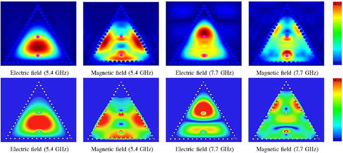
(III) an SIW triangular resonator, also designed on an Arlon CuClad 250GX substrate with a thickness of 1.5 mm and overall dimensions a = 42.0 mm and b = 55.0 mm. It consists of 51 grounded metallic vias, each with a radius of 0.5 mm, uniformly spaced to form an SIW triangular resonator with an effective base length of 36.0 mm and an effective height of 48.0 mm. The resonator is fed by two 50 Ω coaxial probes, both located at the midpoint along dimension a (i.e., at a/2 with respect to the x-axis). Along dimension b (the y-axis), probe P1 is positioned 6.0 mm away from the nearest SIW wall (the triangle base), while probe P2 is located 16.0 mm away from P1. The analysis is carried out over the frequency range from 4.0 to 9.0 GHz. The resonator geometry is shown in Fig. 6 (a), while the magnitude of the S-parameters, calculated using both CAPC and HFSS, is presented in Fig. 6 (b). Furthermore, the electric and magnetic fields at 5.4 GHz and 7.7 GHz are depicted in Fig. 7.


Electric and magnetic fields within the triangular SIW resonator computed with CAPC (top) and HFSS (bottom).
(IV) an SIW circular resonator, also designed on an Arlon CuClad 250GX substrate with overall dimensions a = 55.0 mm and b = 55.0 mm. It consists of 72 grounded metallic vias, each with a radius of 0.5 mm, uniformly spaced to form an SIW circular resonator with a radius of 25.0 mm. The resonator is fed by two 50 Ω coaxial probes, both located at the midpoint along dimension a. Along dimension b, probes are positioned 11.5 mm away from the SIW wall. The analysis is carried out over the frequency range from 4.0 to 10.0 GHz. The resonator geometry is shown in Fig. 8 (a), while the magnitude of the S-parameters is presented in Fig. 8 (b). Furthermore, the electric and magnetic fields at 4.8 GHz and 9.3 GHz are depicted in Fig. 9.


Electric and magnetic fields within the circular SIW resonator computed with CAPC (top) and HFSS (bottom).
In the analysis of structures based on SIW walls, special attention must be paid to the number of metallic vias used to emulate an equivalent metallic wall. With the proposed model, the following strategy can be adopted: the number of metallic pins in the SIW geometry can be increased until the electromagnetic field outside the SIW walls becomes negligible. As a practical guideline, an initial pin spacing of approximately λ/10 can be used.
These analyses demonstrate that the proposed CAPC tool is highly efficient for computing the properties of SIW devices. In all cases, the simulation time was on the order of a few tens of seconds, whereas HFSS required several tens of minutes. In addition, the accuracy of CAPC is remarkable, as evidenced by the excellent agreement between the S-parameters obtained with CAPC and HFSS. Quantitatively, for the analyzed cases, a deviation smaller than 1% was observed when comparing CAPC with HFSS, along with no significant variation in the magnitude of the S-parameters. A similarly strong agreement was also observed for the electric and magnetic field distributions calculated by both tools. Hence, the proposed model is thoroughly validated and can be applied not only for preliminary design but also for the full design of SIW devices with different geometries. The program runs efficiently on a personal computer without requiring significant processing or memory resources. For this study, the implementation was carried out in MATLAB using a matrix-based strategy to optimize the code, as discussed in [15]. The flowchart describing the CAPC implementation is shown in Fig. 10. Except for the frequency loop, all other computations, including the double summations, are performed using matrix operations.

With respect to the metallic posts inserted through the dielectric substrate, they can be classified into two groups: those forming the walls of the resonant cavities and those responsible for perturbing the cavity and modifying its shape. Variations in the radii of the posts forming the sidewalls directly affect the effective dimensions of the SIW structure [5], [6], [7], [8], [9]. Larger radii reduce the effective dimensions, leading to higher resonant frequencies for the unperturbed cavity, whereas smaller radii produce the opposite effect.
For the second group, namely the perturbing posts, thinner cylinders or prisms—as considered in this work—tend to decrease the operating frequency, while thicker elements increase it, resulting in a shift of the resonant frequency. This behavior arises from the shape perturbations introduced by the metallic posts connecting the top and bottom walls, which modify the distribution of stored electric and magnetic energies within the cavity. From a circuit perspective, thinner prisms exhibit higher equivalent inductance, whereas thicker prisms exhibit lower inductance, thereby loading the resonator differently and altering its response [13], [14], [15], [16].
III. Design of C-Band Band-pass Filters Based on Coupled Resonant Cavities
This section provides a guideline for designing a band-pass filter based on coupled resonant cavities. The methodology used here is adapted from [10], and applied to SIW filters. First, the design procedure is outlined, beginning with the selection of the operating frequency and ending with the determination of the filter dimensions. Next, the procedure is applied to the design of a C-band band-pass filter. The resulting dimensions are used in the CAPC to evaluate its performance and refine its characteristics, with the goal of improving the preliminary results. With the filter characteristics computed using the CAPC, the design was implemented in HFSS to assess its performance with a full-wave electromagnetic simulator. Finally, a prototype of the filter was manufactured, and its scattering parameters were measured with a vector network analyzer.
A. Band-pass filter design
The band-pass filter is composed of n associated resonant cavities, where n is the order of the filter. Each cavity has a length lj, delimited by a pair of metallic posts separated by a distance dj, as depicted in Fig. 11. The parameters lj and dj must be determined according to the steps presented below.

The first step is to define the center frequency. Using a standard waveguide dimension table, the filter width, a, can be determined. The filter center frequency must fall within the recommended waveguide frequency range, and the effective width should be corrected by the factor . Next, the desired filter specifications are established, such as bandwidth, order, and insertion-loss ripple. Based on the chosen bandwidth, the guided-wavelength fractional bandwidth, ωλ, can be calculated as:
where are the guided wavelengths at the center frequency, the lower cutoff frequency, and the upper cutoff frequency, respectively.
Once defined the filter order and ripple, the parameters (g0, g1, ..., gj+1), which correspond to the Chebyshev coefficients, can be calculated using closed-form equations or obtained from tables available in [10]. The filter order defines the number of resonant cavities within the structure. Then, the inverter parameters Kj,j+1/Z0, and normalized reactances Xj,j+1/Z0 are calculated using the following equations:
After defining the normalized reactances, the electrical length of each cavity, θj, and its physical length, lj, are determined by the following expressions:
The distances dj are determined directly from graphics present on [10] using the normalized reactances. Finally, the probe positions may be obtained using the CAPC, according to the desired filter response.
The C-band band-pass filter presented here was designed as a third-order filter with center frequency of 5.6 GHz, a bandwidth of 200 MHz, and an insertion loss ripple of 0.1 dB. A substrate with dielectric constant εr = 2.6, loss tangent δd = 0.022, and height h = 1.524 mm was considered. After applying the described methodology and optimizing the circuit with the CAPC to adjust the positions of the metallic vias and coaxial probes, the final structure shown in Fig. 12 (a) was obtained, with dimensions a = 24.60 mm and b = 73.51 mm, and the positions of the coaxial probes (p1 e p2) and perturbations (vn) summarized in Fig. 12 (b). The SIW walls are made up of 38 metallic vias uniformly distributed according to Fig. 12 (a). Due to the symmetrical nature of the circuit, only the positions of selected pins and probes are shown in detail.

The filter was then implemented in the HFSS to validate the results. Further optimization was performed, and the updated positions of the coaxial probes and metallic posts are given in Fig. 12 (b). The final width and length are a = 25.40 mm and b = 73.51 mm, respectively.
The scattering parameters and group delay of the filter show good agreement between the results predicted by CAPC and those obtained with HFSS, as illustrated in Fig. 13 (a) and Fig. 13 (b), respectively. In addition, the electric and magnetic field distributions, obtained with CAPC (Fig. 14 (a) and Fig. 14 (b)) and HFSS (Fig. 14 (c) and Fig. 14 (d)), are shown. Although some differences in the final dimensions of the filter were observed, the CAPC has proven to be a valuable tool for the initial stage of the design process.


Electric and magnetic fields within the C-band band-pass filter: (a) electric field and (b) magnetic field computed with CAPC; (c) electric field and (d) magnetic field computed with HFSS.
B. Prototype
To validate the design presented in the previous subsection, a prototype was fabricated at the LAP/ITA facilities, using the geometry optimized in the HFSS (Fig. 12). Its experimental performance was then compared with the results obtained from CAPC and HFSS. The circuit was built on an Arlon CuClad 250 GX dielectric substrate with a thickness of 1.524 mm. Copper removal, drilling, and cutting, illustrated in Fig. 15 (a), were carried out using a T-Tech AMC-2500 milling machine. Fig. 15 (a) also illustrates Kapton tape insulation used to facilitate pin soldering. After soldering the copper-made pins and the SMA connectors, the final SIW filter circuit is shown in Fig. 15 (b) (bottom view) and Fig. 15 (c) (top view).

Prototype of the C-band bandpass filter: (a) substrate with holes, (b) filter: bottom view, (c) filter: top view, and (d) measurement setup.
Next, the scattering parameters and group delay were measured using an E5071C ENA Vector Network Analyzer in the setup shown in Fig. 15 (d). Owing to the reciprocity of the circuit, only S11, S21, and the group delay were considered in the filter analysis. The results show excellent agreement between the theoretical predictions and the experimental data, as illustrated in Fig. 16 (a) and Fig. 16 (b). The small deviations observed can be attributed to uncertainties in the fabrication process and to the tolerances of the dielectric substrate’s permittivity. The measured group delay is typically noisy due to the phase characteristics of S21; therefore, a filtering procedure was applied to the group-delay data to suppress this undesired effect. Finally, due to this excellent agreement between the measurements and the CAPC predictions, the proposed model has been successfully validated.

Curves of S-parameter and group delay comparing the analytical model, simulation, and prototype: (a) magnitude of the S-parameter and (b) group delay.
IV. Conclusions
This work presents the evolution of the efficient computational tool CAPC for the analysis of SIW circuits. CAPC was adapted to analyze N-port perturbed planar circuits shielded by SIW walls. In the analysis of SIW devices, CAPC requires significantly less memory and considerably shorter processing time than commercial software, thereby enhancing the design of perturbed SIW cavities. In addition to computing the S-parameters and their derived properties, the proposed model also calculates the internal electric and magnetic fields, enabling the user to assess the quality of the implemented SIW walls and to determine the best compromise between the number of pins and the accuracy of the synthesized metallic wall.
As future improvements, CAPC can be integrated with evolutionary algorithms to optimize SIW geometries that meet user-defined transfer functions. Another possibility is the use of CAPC for the design of other SIW circuits, such as power dividers, directional couplers, and antenna-array beamformers. There are also possibilities for designing reconfigurable SIW circuits based on PIN diodes, varactor diodes, and MEMS switches, which could be further assisted by the aforementioned evolutionary algorithms.
Acknowledgments
The authors acknowledge the CNPq – National Council for Scientific and Technological Development for the financial support (Grants 305944/2023-1 and 405889/2021-6).
Data Availability
The data that support the findings of this study, including simulation and measurement results, are available from the corresponding author, Ricardo C. Caleffo, upon reasonable request.
REFERENCES
- 1 J. Lee, E. Tejedor, K. Ranta-aho, H. Wang, K.-T. Lee, E. Semaan, E. Mohyeldin, J. Song, C. Bergljung, and S. Jung, “Spectrum for 5g: Global status, challenges, and enabling technologies,” IEEE Communications Magazine, vol. 56, no. 3, pp. 12–18, 2018.
- 2 I.-P. Belikaidis, A. Georgakopoulos, E. Kosmatos, V. Frascolla, and P. Demestichas, “Management of 3.5-ghz spectrum in 5g dense networks: A hierarchical radio resource management scheme,” IEEE Vehicular Technology Magazine, vol. 13, no. 2, pp. 57–64, 2018.
- 3 D. M. Pozar, Microwave Engineering, 4th ed. Hoboken, NJ: Wiley, 2012.
- 4 S. Ramo, J. R. Whinnery, and T. V. Duzer, Fields and Waves in Communication Electronics, 3rd ed. Hoboken, NJ: John Wiley & Sons, 1994.
- 5 X.-P. Chen and K. Wu, “Substrate integrated waveguide filter: Basic design rules and fundamental structure features,” IEEE Microwave Magazine, vol. 15, no. 5, pp. 108–116, 2014.
- 6 M. Bozzi, A. Georgiadis, and K. Wu, “Review of substrate-integrated waveguide circuits and antennas,” Microwaves, Antennas ’I&’ Propagation, IET, vol. 5, pp. 909 – 920, 2011.
- 7 K. Wu, M. Bozzi, and N. J. G. Fonseca, “Substrate integrated transmission lines: Review and applications,” IEEE Journal of Microwaves, vol. 1, no. 1, pp. 345–363, 2021.
- 8 F. Xu and K. Wu, “Guided-wave and leakage characteristics of substrate integrated waveguide,” IEEE Transactions on Microwave Theory and Techniques, vol. 53, no. 1, pp. 66–73, 2005.
- 9 D. Deslandes and K. Wu, “Accurate modeling, wave mechanisms, and design considerations of a substrate integrated waveguide,” IEEE Transactions on Microwave Theory and Techniques, vol. 54, no. 6, pp. 2516–2526, 2006.
- 10 G. L. Matthaei, L. Young, and E. M. T. Jones, Microwave Filters, Impedance-Matching Networks, and Coupling Structures. McGraw-Hill, 1964.
- 11 K. Entesari, A. P. Saghati, V. Sekar, and M. Armendariz, “Tunable siw structures: Antennas, vcos, and filters,” IEEE Microwave Magazine, vol. 16, no. 5, pp. 34–54, 2015.
- 12 P. Liu, Z. Li, W. Fu, J. Yin, X. Qiu, and T. Ye, “Complementary split-ring resonators in microwave filters: A review and focus on structural progress,” IEEE Microwave Magazine, vol. 23, no. 9, pp. 70–84, 2022.
- 13 R. C. Caleffo and F. S. Correra, “A novel and compact 3.5 ghz tunable bandpass filter in siw technology with shunt-inductive discontinuities switched by pin diode switches,” Microwave and Optical Technology Letters, vol. 63, no. 2, pp. 471–479, 2021.
- 14 R. C. Caleffo, “Determining a perturbation factor to design tunable resonant cavities in siw technology,” Journal of Microwaves, Optoelectronics and Electromagnetic Applications, vol. 22, no. 1, pp. 230–242, 2023.
- 15 R. C. Caleffo, D. C. do Nascimento, and D. B. Ferreira, “An accurate closed-form formulation for analyzing perturbed planar cavities,” IEEE Transactions on Microwave Theory and Techniques, vol. 73, no. 8, pp. 4579–4587, 2025.
- 16 R. C. Caleffo, M. H. Seko, and F. S. Correra, “A novel electronically tunable siw cavity with wide discrete frequency variation using dual-mode perturbation,” Microwave and Optical Technology Letters, vol. 67, no. 8, pp. 1–9, 2025.
- 17 Y. Lo, D. Solomon, and W. Richards, “Theory and experiment on microstrip antennas,” IEEE Transactions on Antennas and Propagation, vol. 27, no. 2, pp. 137–145, 1979.
- 18 W. Richards, Y. Lo, and D. Harrison, “An improved theory for microstrip antennas and applications,” IEEE Transactions on Antennas and Propagation, vol. 29, no. 1, pp. 38–46, 1981.
- 19 W. F. Richards and Y. T. Lo, “Theoretical and experimental investigation of a microstrip radiator with multiple lumped linear loads,” Electromagnetics, vol. 3, no. 4, pp. 371–385, 1983.
- 20 E. dos Santos Silveira, F. Antreich, and D. C. do Nascimento, “Frequency-reconfigurable siw microstrip antenna,” AEU - International Journal of Electronics and Communications, vol. 124, pp. 1–9, 2020.
- 21 F. F. Oliveira, J. M. Vieira, D. B. Ferreira, and D. C. Nascimento, “Improved model for microstrip antennas loaded by metallic vias with lumped elements,” International Journal of Microwave and Wireless Technologies, vol. 17, no. 1, p. 140–148, 2025.
- 22 R. F. Harrington, Time-Harmonic Electromagnetic Fields. IEEE Press, 2001.
- 23 R. Garg, P. Bhartia, I. Bahl, and A. Ittipiboon, Microstrip Antenna Design Handbook. Boston, London: Artech House, 2001.
- 24 R. F. Harrington, Field Computation by Moment Methods. Piscataway, NJ: IEEE Press, 1993.
-
Editor:
Carlos E. Capovilla
-
Associate Editor:
Karcius D. R. Assis