Calculation of the equivalent circuit for a plastic film capacitor intended for DC-link application in power electronic converters
ABSTRACT
Capacitor designs employed in DC-link applications of power electronic converters must minimize equivalent series resistance and parasitic inductance due to the adoption of wide bandgap semiconductors, which enable operation at significantly higher temperatures, voltages, and switching frequencies. The paper focuses on characterizing metallized plastic film capacitors by analyzing the influence of materials, dimensions, and construction features, both of the capacitive element and of the connections and terminals, on parasitic inductance and associated losses, thereby supporting the development of an equivalent circuit model. A comprehensive literature review establishes the theoretical foundation for the analytical formulation, which is then applied to the structural characteristics of the capacitor under investigation to derive the parameters of the equivalent circuit. The calculated values of equivalent series inductance and equivalent series resistance are validated through comparison with measurements obtained from different capacitor models. The results confirm the accuracy of the proposed calculation method, as the observed deviations remain within acceptable limits, considering the inherent variability of raw materials, manufacturing processes, and measurement procedures.
KEYWORDS
Metallized plastic film capacitor; Equivalent circuit of the capacitor; Equivalent series inductance; Equivalent series resistance
I. INTRODUCTION
The use of wide bandgap (WBG) semiconductors, including those manufactured with silicon carbide (SiC), has already become a reality as a replacement for their silicon (Si) counterparts, enabling operation at significantly higher temperatures, voltages, and switching frequencies. These types of semiconductors make power electronics modules more powerful and energy-efficient, driving advancements in energy processing for automotive electric traction and renewable energy applications such as solar and wind. However, the increase in switching frequency raises the levels of current and voltage derivatives (di/dt and dv/dt) over time, making the system more susceptible to parasitic elements such as inductors and capacitors [1], [2].
Thus, in order to keep pace with the advancement of semiconductors, the other components that constitute the power modules of static converters must also evolve. One of the main components involved in this process is the capacitor applied to the DC-Link of the converter. The equivalent series inductance (ESL) present at the semiconductor terminals is primarily responsible for voltage spikes during the turn-off event, and these spikes can lead to premature failures in both the semiconductors and the capacitor. The inductances of the capacitor and the connection busbars significantly contribute to this parasitic inductance; therefore, they must be minimized to reduce the impact on the circuit [3], [4], [5].
With the trend toward higher switching frequencies, it is essential to reduce parasitic inductance and, consequently, the inductance of the DC-link capacitor [6]. Additionally, as switching frequency increases, switching losses also rise, and combined with higher operating temperatures, capacitor losses must be minimized to maintain the maximum hotspot temperature within acceptable limits for proper functionality, according to product design specifications. Achieving these improvements in capacitor performance requires detailed knowledge of its characteristics and how each component impacts parasitic inductance and losses, enabling the identification of the most suitable product design for the intended application.
Several studies and papers address this topic, aiming to quantify capacitor losses and parasitic inductance. However, since equivalent circuit analysis is highly dependent on product design and application, evaluations are often specific to the capacitor model under investigation. In [7], a comprehensive approach is presented for both losses and ESL, but applied to low-power capacitors with cable connections. In [8], a distributed circuit model is evaluated for inductance calculation, but applicable to stacked multilayer capacitors. In [3], an equivalent circuit model for metallized plastic film capacitors is developed and adjusted based on comparisons between model and measurements, though without analytical formulation of the components. In [9], the calculation of self and mutual inductance of line filter capacitors is carried out; thus, the analysis is performed for frequencies above the resonance frequency. In [10], a distributed equivalent circuit for capacitor representation is presented; however, not all components are calculated, as some are defined based on measurements.
Aiming to mitigate these gaps, this paper seeks to map the capacitor and to quantify the influence of materials, dimensions, and design, both of the capacitive element and of the connections and terminals, on parasitic inductance and losses. Based on this analysis, the goal is to develop the calculation of the components of the capacitor equivalent circuit, during the project design phase, while the electrical and mechanical characteristics are being established, supporting evidence-based choices regarding cost–benefit performance, without the need for prototype manufacturing.
This paper is derived from specific constructive characteristics, and no equivalent literature was found to enable a comparison of results. Therefore, the evaluation of the analytical model is carried out experimentally by comparing calculated and measured values.
II. METALLIZED PLASTIC FILM CAPACITOR
Metallized plastic film capacitors are suitable for high-power applications at low and medium voltage levels due to their low losses and high reliability [6].
A. METALLIZED PLASTIC FILM
The metallized plastic film consists of a base film, which forms the capacitor dielectric and is typically made of polypropylene (PP), polyethylene terephthalate (PET), polyethylene naphthalate (PEN), or polyphenylene sulfide (PPS), with a thickness on the order of a few micrometers. The base film is coated on one side with a thin metal layer, with a thickness on the order of a few nanometers, generally composed of an aluminum base with an overlaid zinc layer [7], [11], [12].
Although metallization profiles may vary, they follow a standard configuration consisting of: a heavy edge, located at one end of the base film width and characterized by greater thickness; a free margin, located at the opposite end of the base film width and without metallization; and an active area, which lays between the heavy edge and the free margin and has a smaller thickness compared to the heavy edge [7]. The representation of the metallized film is shown in Fig. 1.

To characterize the film metallization profile, the electrical property of surface resistivity is used, which corresponds to the resistance between two parallel surfaces of a square, independent of the area of the square. The measurement of the surface resistivity is expressed in ohms per square (Ω/□) [7], [13].
The metallization profile develops along the width of the metallized film. Along its length, the profile remains constant, simply replicating the configuration observed across the width.
B. CAPACITIVE ELEMENT
The capacitive element consists of a plastic core, whose diameter may vary depending on the application, around which two metallized films are wound in parallel. The metallized layer of the second film is positioned in contact with the non-metallized side of the first film. The films are arranged so that their heavy edges are on opposite sides, making each end of the capacitive element correspond to one pole (electrode) of the capacitor. Additionally, an axial offset is applied between the films, with the heavy edge slightly elevated to improve the electrical contact between the metallized layer and the external connection and to enhance electrical insulation between films of opposite polarities [7].
After winding the metallized films, a zinc coating is deposited on both ends of the capacitive element (end-spray). This coating, composed of zinc grains, serves to interconnect all turns of the metallized film with the same polarity and to provide a base for the electrical connection to the capacitor terminals [7].
The calculation of the capacitor’s metallized film length is based on the capacitance equation, considering that the capacitor electrodes are arranged in a stacked configuration [14], [15]. The length of the metallized film is determined according to (1).
where is the film length (m); is the capacitance (F); is the base film thickness (m); is the vacuum permittivity (F/m); is the relative permittivity of the dielectric; is the film width (m); is the free margin of the film (m); and is the offset between films (m).
After calculating the film length, the external diameter of the capacitive element can be determined. The external diameter is given by (2).
where is the external diameter of the capacitive element (m); and is the core diameter (m).
The height of the capacitive element is calculated as shown in (3).
where is the height of the capacitive element (m).
C. ASSEMBLED CAPACITOR
The capacitive element forms the core of the capacitor, as it comprises the dielectric and the electrodes. However, the electrical connection between the capacitive element and the external part of the capacitor is established through cables, strips, and busbars, while the terminals are responsible for supplying electrical power to the capacitor. Consequently, their structure is closely related to the product’s intended application.
III. EQUIVALENT CIRCUIT
The approach for analyzing and calculating the capacitor equivalent circuit varies significantly with changes in product design, particularly regarding the evaluation of parasitic inductance, due to the geometry of the components and the interaction between them. Capacitors for power electronics, applied in DC-link configurations of converters, offer a wide range of constructive possibilities. Therefore, for the development of this paper, the following design characteristics are considered, which are widely employed in DC‑link capacitors:
-
Non-segmented metallization profile without series-connected capacitors.
-
Double-end circular capacitive element, where the electrodes are connected on opposite sides.
-
Two metallized films with identical characteristics in width, base film thickness, and free margin.
-
Radial feed, with terminals positioned on the same side.
-
Electrical connection through strips.
-
Female screw terminal with cylindrical body and hexagonal base.
The capacitive elements, electrical connections, and terminals constitute the components considered in the evaluation of the capacitor equivalent circuit. This analysis will be carried out in two stages: first, the assessment of losses through the equivalent series resistance (ESR), and subsequently, the evaluation of parasitic inductance through the ESL.
A. EQUIVALENT SERIES RESISTANCE
For the capacitive elements, the analysis is based on a distributed equivalent circuit model, considering only the resistance and capacitance of the circuit, which allows representing the multiple layers that compose the capacitor. A simplified representation of the distributed equivalent circuit is shown in Fig. 2, where R denotes the surface resistivity of the metallized layer and C represents the capacitance between two consecutive electrodes within the analyzed area. It is observed that the capacitance is multiplied by two, which occurs due to the stacking of metallized film layers [7].

To ensure that the distributed equivalent circuit accurately represents the capacitor, it must be correlated with its physical structure. Fig. 3 illustrates the division of the metallized film into small square areas, referred to as mini-squares. Based on the analysis of the electrical characteristics of these mini-squares, the distributed equivalent circuit is developed [7].

For the development of this paper, a circuit model with a central resistor is used, where the capacitors are positioned at the ends and the resistors in the central regions of the subcircuits. In this circuit model, the beginning and the end of the metallized film are composed of half of a mini-square, causing the first and the last capacitors in the circuit to have half the capacitance of the other capacitors [7].
The accuracy of the distributed equivalent circuit, which represents a continuous physical structure, increases as the number of mini-squares composing it grows [7]. The circuit was divided into fifteen mini-squares, as this quantity yielded satisfactory results in the analyses presented in [7]. Fig. 4 shows the circuit, where R1 to R15 correspond to the surface resistivity of the metallization of the first film, R16 to R30 correspond to the surface resistivity of the metallization of the second film, and C1 to C16 correspond to the capacitance in the area formed by the mini-square, noting that C1 and C16 have half the capacitance of the other capacitors in the circuit. Components R1 to R30 and C1 to C16 represent the region where there is overlap between the two films, and to represent the surface resistivity of the film ends, where there is no overlap, components Rsa and Rsb were added.
The mini-square dimensions are calculated based on the region where the films overlap, as described in (4).
where is the mini-square dimension (m).
The distributed equivalent circuit represents the capacitor along the width of the metallized film, and to replicate it along the length of the film, it is necessary to calculate the number of mini-squares along the length, as shown in (5) [7].
where is the number of mini-squares along the length of the film.
The resistance values of R1 to R15 and R16 to R30 depend on the designed metallization profile of the films. Therefore, it is necessary to define the position of each resistor relative to the width of the films, starting from the heavy edge, as presented in (6) and (7) for the first film.
where is the position of R1 on the film (m); and is the position of R2 on the film (m).
The calculation of the positions of resistors R3 to R15 is performed successively, as shown in (7).

The positions of resistors R16 to R30 in the second film follow the same approach, considering that R30 is located at the heavy edge, as occurs with R1 in the first film. Therefore, the position of resistor R30 is equal to that of R1, the position of R29 is equal to that of R2, and so on.
The resistance values of resistors Rsa and Rsb are defined based on the relationship between the regions located at the ends of the films and the mini-square dimensions, where there is no overlap, considering the surface resistivity of this region equal to the designed resistivity of the heavy edge, as presented in (8).
where is the resistance at the end of the first film (Ω); is the resistance at the end of the second film (Ω); and is the surface resistivity of the heavy edge (Ω/□).
The capacitance values of capacitors C2 to C15 correspond to the capacitance of each mini-square and depend on its area relative to the total electrode area of the capacitive element. The capacitance values of capacitors C1 and C16 are half the capacitance of a mini-square, as previously mentioned. The calculation of the mini-square capacitance is given by (9) [7].
where is the capacitance of the mini-square (F); and is the total designed capacitance of the element (F).
After defining all components of the distributed equivalent circuit, the calculation of the equivalent impedance is performed. From the circuit equivalent impedance, it is possible to obtain equivalent capacitance and equivalent resistance. The total capacitance of the capacitive element and the total series resistance of the metallization of the metallized plastic film can be calculated by considering the presence of multiple parallel circuits along the length of the films, as presented in (10) and (11) [7].
where is the total capacitance of the capacitive element (F); is the equivalent capacitance of the distributed equivalent circuit (F); is the total series resistance of the metallization of the plastic film (Ω); and is the equivalent resistance of the distributed equivalent circuit (Ω).
The capacitor dissipation factor (DF) is the ratio between active power and reactive power, or, more simply, the ratio between the ESR and the capacitive reactance of the capacitor. The ESR consists of dielectric losses and conductor losses, such as those in terminals, connections, end-spray, and metallization of the plastic film (electrodes). Dielectric losses can be represented by a resistance that should be inversely proportional to frequency, since at low frequencies these losses are predominant compared to conductor losses. Therefore, dielectric losses can be calculated according to (12) [7], [11].
where is the resistance representing dielectric losses (Ω); is the resistive component of dielectric losses (Ω); is the frequency (Hz); and is the dielectric dissipation factor at low frequencies.
Equation (12) is applicable in situations where the dielectric exhibits a constant dissipation factor at low frequencies, as is the case for polypropylene film [7].
The resistance of the end-spray, which connects the multiple turns of the film, depends on the contact area with the metallization of the plastic film, with the worst case occurring when the zinc grains only contact the film metallization through its thickness [14]. However, due to the offset between the films, there is penetration of grains between them, increasing the contact area with the film metallization. Since the penetration depth of the grains in the offset region is not uniform, penetration in half of this region is considered for calculation purposes.
To calculate the thickness of the heavy edge of the metallized film layer, the metallization pattern is assumed to be made of aluminum and zinc at the heavy edge, while the active area consists only of aluminum, represented by the extended-edge metallization profile. Based on the resistivity data of the heavy edge and the active area, the thicknesses of the aluminum and zinc layers, and the total thickness of the heavy edge are determined employing (13), (14) and (15) [14].
where is the thickness of the aluminum layer (m); is the aluminum resistivity (Ω·m); is the surface resistivity of the active area (Ω/□); is the thickness of the zinc layer (m); is the zinc resistivity (Ω·m); and is the thickness of the heavy edge (m).
The end-spray resistance (18) consists of the surface resistance, formed by the contact between zinc grains and the thickness of the heavy edge of the film metallization (16), and the resistance resulting from the penetration of zinc grains into the offset region between films (17) [14].
where is the surface resistance of the end-spray (Ω); is the end-spray thickness (m); is the resistance due to the penetration of zinc grains into the offset region between films (Ω); and is the total resistance of the end-spray (Ω).
The series resistance of the capacitive element is calculated according to (19), and the ESR of the capacitive element is calculated according to (20) [7], [14].
where is the series resistance of the capacitive element (Ω); and is the equivalent series resistance of the capacitive element (Ω).
The calculation of the connection strips and terminal resistances is based on Ohm’s Second Law.
For the connection strips, the resistance is calculated according to (21).
where is the strip resistance (Ω); is the material resistivity (Ω·m); is the strip length (m); is the strip width (m); and is the strip thickness (m).
The terminal considered is as shown in Fig. 5, and its resistance is calculated according to (22).

where is the terminal resistance (Ω); is the height of the threaded region (m); is the diameter of the cylindrical region (m); is the diameter of the threaded region (m); is the height of the cylindrical region (m); is the height of the hexagonal region (m); and is the width of the hexagonal region (m).
After calculating the ESR of the capacitive elements and the resistances of the connection strips and terminals, the ESR of the capacitor can be determined. The equivalent circuit used for this calculation depends on the number of capacitive elements and the connection configuration, which are design parameters.
B. EQUIVALENT SERIES INDUCTANCE
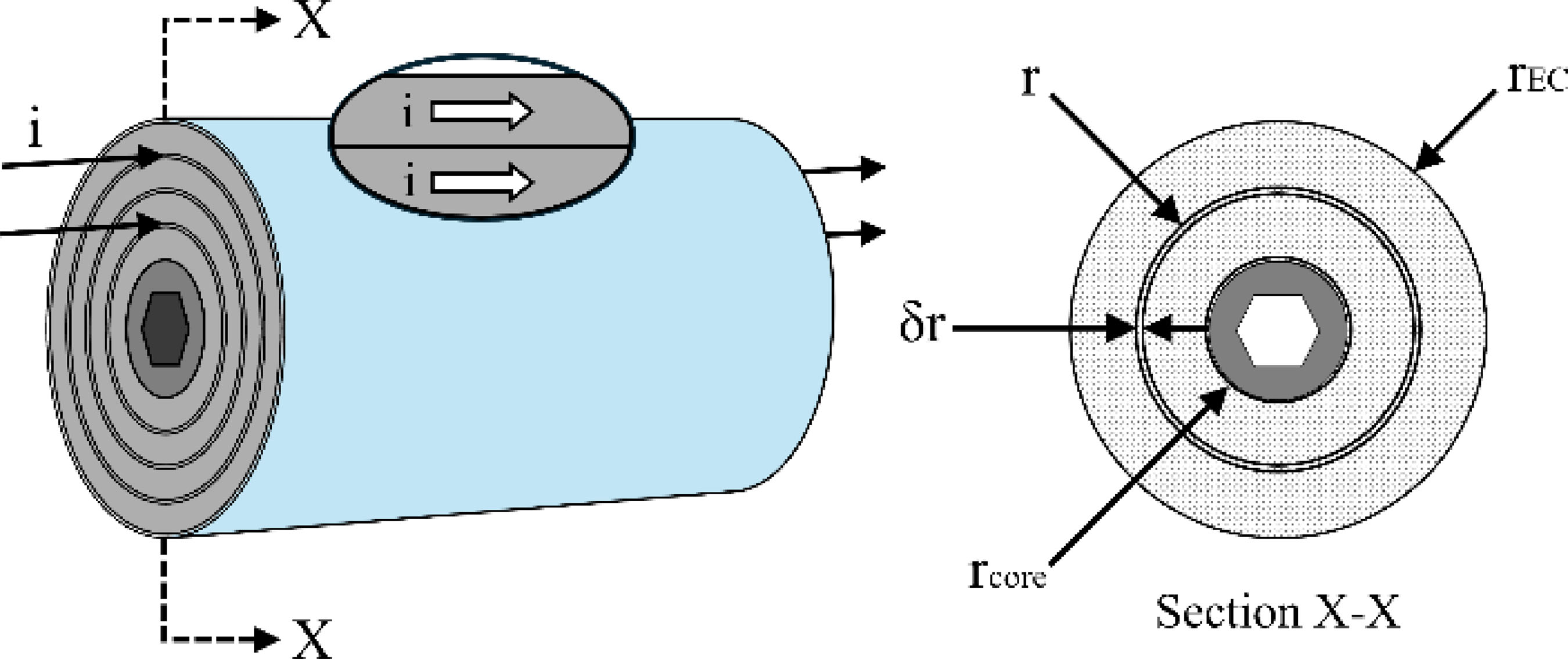
The current flows through the capacitive element in two ways: radially, via the end-spray, and longitudinally, via the film metallization. Considering a uniform distribution of current in the radial direction, no magnetic field, and consequently no inductance is generated [16].
In this paper, a circular capacitive element with double-end is considered, where the electrodes are connected on opposite sides. Thus, the currents in both electrodes flow in the same direction, as shown in Fig. 6. The longitudinal current, which flows through the plastic film metallization, induces a magnetic field and this generates parasitic inductance [7], [16].

Using Ampère’s Law as the basis for calculating the magnetic field intensity generated by the electric current flowing through the turns of the metallized film, and evaluating the electromagnetic energy stored in these turns,
the equation for parasitic inductance per unit height of the capacitive element is obtained. When multiplied by its height, this becomes the parasitic inductance of the capacitive element, as given in (23) [7], [16].
where is the parasitic inductance of the capacitive element (H); is the magnetic permeability of the medium (H/m); is the outer radius of the capacitive element (m); and is the core radius (m).
The electrical connections considered in this paper are flat
strips; therefore, the calculation of the strip self-inductance is similar to the calculation of busbar self-inductance, as presented in [17] and shown in (24).
where is the strip self-inductance (H); is the magnetic permeability of vacuum (H/m); and is the relative magnetic permeability of the medium.
The capacitor terminals, due to their design with a cylindrical body and hexagonal base, do not exhibit significant inductance and were therefore disregarded in the calculation.
Inductance arises from the interaction energy between electrical circuits, being referred to as self-inductance when it depends on the energy of the circuit itself, as previously evaluated, and as mutual inductance when there is interaction between different circuits [18].
For calculating the parasitic inductance of the capacitor, mutual inductances between overlapping or adjacent connection strips and between connection strips and capacitive elements are considered.
The calculation of mutual inductance between overlapping connection strips, similar to what occurs in self-inductance, is equivalent to the calculation of mutual inductance between busbars, as presented in (25) [17].
where is the mutual inductance between overlapping strips (H); is the overlapping length of the strip (m); is the distance between strips (m); and is the correction factor, which depends on the interaction between strips.
The calculation of mutual inductance between adjacent connection strips depends on their spatial positioning [18]. For this paper, the mutual inductance between two connection strips arranged in a ‘V’ configuration, with an angle θ between them, is evaluated.
Using Neumann’s formula, which calculates the mutual inductance of two closed circuits carrying current and positioned arbitrarily in space, and considering that the two strips in the ‘V’ configuration have the same length and that the analysis is performed at the midpoint of each strip, is obtained the mutual inductance between the strips ( (26) [18].
The calculation of mutual inductance between the capacitive element and the connection strip is performed using Faraday’s Law, where mutual inductance is the proportionality constant between the magnetic flux generated by the first conductor that crosses the second conductor. In this way, it is possible to calculate the mutual inductance in the connection strip induced by the capacitive element (27) and the mutual inductance in the capacitive element induced by the connection strip (28) [19]. In the case of mutual inductance in the capacitive element, since the area crossed by the magnetic flux generated by the connection strip is not solid, being formed by layers of metallized plastic film, a factor of 3×10⁻³ is considered in the calculation, representing the ratio between the metallized (conductive) area and the plastic (dielectric) area.
where is the mutual inductance in the connection strip induced by the capacitive element (H); is the angle between the magnetic induction vector and the interest area (°); is the length of the interest area (m); is the maximum distance from the center of the capacitive element within the region covered by the connection strip (m); is the minimum distance from the center of the capacitive element within the region covered by the connection strip (m); is the mutual inductance in the capacitive element induced by the connection strip (H); is the maximum distance from the center of the connection strip within the region covered by the capacitive element (m); and is the minimum distance from the center of the connection strip within the region covered by the capacitive element (m).
After formulating the self and mutual inductances, the calculation of the LSE of the capacitor depends on its structure and the positioning of the connection strips relative to the capacitive elements. The impact of mutual inductance on the equivalent inductance depends on the direction of the currents in the conductors under analysis; that is, if both conductors carry currents in the same direction, the mutual inductance is added to the self-inductance. However, if the currents flow in opposite directions, the mutual inductance is subtracted from the self-inductance [17].
IV. CAPACITOR DESIGN
In the initial phase of capacitor design, input data are received, consisting of nominal capacitance, voltage and current, dimensions, and application type. Based on these input data, the electrical and mechanical characteristics of the capacitor are defined, making it possible to design its detailed structure and calculate the equivalent circuit.
For this paper, the use of metallized film with an extended-edge metallization profile is standardized, with a resistivity of 3 Ω/□ at the heavy edge and 55 Ω/□ in the active area.
To perform the equivalent circuit calculation and subsequently compare it with measured values, six different capacitor models were selected, which already have defined electrical and mechanical characteristics. These characteristics were supplied by the manufacturers of the metallized films and the capacitors and are presented in Table I.
The calculations are performed, assuming a temperature of 20 °C, and for the ESR calculation, a frequency of 1 kHz, with the aim of simulating the measurement environment that underpins the experimental results.
The six selected models consist of one of the basic structures shown in Fig. 7. The base film material is polypropylene, the strips are made of copper, and the terminals are made of brass.

Constructive structure: capacitor with one capacitive element (left) and with two capacitive elements (right).
Initially, calculations are performed for the design of the capacitive element, such as film length and diameter and height of the capacitive element. In capacitors with two capacitive elements, the capacitance of each element is half the total capacitance of the capacitor.
Subsequently, the calculation of the ESR of the capacitive elements is carried out, based on the distributed equivalent circuit shown in Fig. 4, along with the resistance of the connection strips, the resistance of the terminals, and the ESR of the capacitor. The latter is calculated using one of the resistive equivalent circuits presented in Fig. 8 and Fig. 9.


After completing the calculation of the ESR of the capacitor, the calculation of the ESL begins. The inductance calculation consists of the self-inductance component and the mutual inductance component, depending on the connection configuration between the strips and the capacitive elements. First, the self-inductances of the capacitive elements and the connection strips are calculated, followed by the mutual inductances: the mutual inductance in ‘V’ between connection strips 1 and 3, the mutual inductances in the strips induced by the capacitive elements, and the mutual inductances in the capacitive elements induced by the strips. Connection strip 2 does not exhibit significant mutual coupling with the capacitive elements; therefore, its mutual inductance is disregarded.
Connection strip 2 has two connection configurations in the evaluated models, as shown in Fig. 10.

In the overlapping-strip configuration (models 1, 2, 3 and 4), the non-overlapping region has a length of 22 mm, and the overlapping region has a length of 19 mm on each side, totaling 60 mm. In this case, in addition to the strip self-inductance, the mutual inductance due to overlap must be considered. Since the overlapping strips are aligned and very close, the correction factor k is considered unity, and the distance between strips is defined as the strip thickness itself.
In the configuration with two separate strips (models 5 and 6), connected in parallel without overlap, the self-inductance of each strip is calculated first, followed by the total parallel self-inductance.
Since the medium surrounding the capacitive elements and the connection strips is composed of insulating material, a relative magnetic permeability of unity is assumed. The distance between strips and capacitive elements is also defined as the thickness of the connection strips themselves.
For strips composed of two parallel parts in full contact without insulation, the calculation of self-inductance considers a single strip with an equivalent thickness equal to the sum of the individual strip thicknesses.
After completing the calculations of self-inductances and mutual inductances, the equivalent inductance of each component is determined, allowing the calculation of the ESL of the capacitor, based on one of the inductive equivalent circuits shown in Fig. 11 and Fig. 12.


The calculated ESR and ESL results of the selected capacitors are shown in Table II.
Based on the equations derived for the capacitor equivalent circuit and the design methodology, an assessment of the project characteristics and their influence on the ESR and ESL results is carried out, as presented in Table III. The evaluation considers constant capacitance, rated voltage, and cross-sectional area of the connection strips, and is based on the constructive structure defined at the beginning of Section III.
The purpose of this paper is to formulate and analyze the capacitor equivalent circuit; therefore, this analysis focuses exclusively on the electrical characteristics, without measuring weight, volume, complexity constructive level, or cost. It is important to note that optimal choices from an electrical standpoint may negatively impact other characteristics, and each case should be evaluated individually.
Analyzing Table III, it can be concluded that increasing the quantity of capacitive elements, the width of the metallized film, and the strip length is detrimental to electrical characteristics of the capacitor, as it raises the ESR and ESL levels. Modifying the core diameter and the thickness and width of the strips, provided the cross-sectional area remains constant, does not affect ESR levels; however, increasing the core diameter and the strip width improves the capacitor performance by reducing ESL. The configuration of strip 2 with parallel connection shows better results, i.e. lower ESR and ESL, when compared to the configuration with overlap.
V. EXPERIMENTAL RESULTS
In order to evaluate and validate the calculation methodology, measurements of the ESR and ESL of the selected capacitor models were performed for subsequent comparison of the results.
Initially, the ESR of the capacitive element of model 4 was measured using a Wayne Kerr impedance analyzer, model 6500B, with the aim of evaluating the ESR behavior over a frequency sweep from 1 kHz to 500 kHz and comparing it with the values calculated as a function of frequency. The comparison between the measured and calculated values is presented in Fig. 13, where agreement between the results can be observed up to 100 kHz. Above this frequency level, distortion appears in the measured values, mainly caused by noise in the measurement system, as well as by the influence of the skin effect and the non-uniform current distribution.

The method used for measuring the ESR of the capacitive element is shown in Fig. 14.

Therefore, the frequency of 1 kHz was adopted for ESR measurements, as this is a frequency commonly used by capacitor manufacturers in datasheets and provides better accuracy in the results.
Subsequently, two assembled units of each model were measured, except for model 3, for which only one assembled unit was measured due to availability constraints. Each unit was measured three times, and the average value was then calculated.
The measurements were carried out at a temperature of 20 °C, representing the standardized ambient temperature [20].
The ESR measurement of the capacitors was carried out using a Wayne Kerr RLC bridge, model 4300, at a voltage of 1 V and a frequency of 1 kHz.
The method used for measuring the ESR and one of the tested capacitors are shown in Fig. 15.

The ESL measurement was performed through a double-pulse test, according to the circuit shown on Fig. 16. The applied voltage was 100 V, the first pulse had a duration of 50 µs and the second pulse of 15 µs, with an interval of 10 µs between them. By obtaining the voltage values and the current variation over time across the capacitor, it is possible to calculate the ESL [21].

The measurements were performed using a Tektronix oscilloscope, model MSO 2024B, with voltage probes and a Rogowski coil.
The method used for measuring the ESL, along with one of the capacitors under test, is shown in Fig. 17. Two overlapping flat busbars are used to connect the capacitor to the test circuit, with the aim of reducing the circuit inductance.

A. COMPARISON OF CALCULATED AND MEASURED VALUES
Table IV presents the comparison between the calculated and measured values of ESR and ESL for the selected capacitors, as well as the variation observed between these values.
For ESR, the calculated values are lower than the measured values, since factors such as solder points are not considered in the calculation.
For ESL, there is a greater fluctuation between measured and calculated values, as in this case there is an influence of self-inductances and mutual inductances that are not accounted for, such as the self-inductance of the terminals and the mutual inductance of connection strip 2 with other components.
The variations between measured and calculated values are considered acceptable, taking into account the normal variability of raw materials and manufacturing processes, as well as the error associated with the measurement procedures. It is noteworthy that, for the ESR, the measured values for the same capacitor showed variations of up to 4.5%, and for the ESL under the same conditions, variations of up to 11.9% were obtained. Therefore, after discounting the inherent measurement inaccuracies, the difference between the measured and calculated values is up to 12% for the ESR and up to 15% for the ESL. These values are considered satisfactory given the complexity of the calculations and the approximations involved.
CONCLUSION
The metallized plastic film capacitor applied in DC-Link of static converters presents several constructive characteristics that impact the ESR and ESL values, with some characteristics being application-dependent and others offering a certain degree of design flexibility.
The formulation of equations that allow the calculation of the capacitor equivalent circuit, based on its constructive characteristics, enables optimal design choices to meet input requirements during the design phase without the need for prototype manufacturing. Furthermore, it allows quantifying the influence of each characteristic on the result.
The validation of the results is carried out through sample measurements, and the comparison between calculated and measured values demonstrates that the calculation method is effective, as the variations are within acceptable limits, considering the normal variability of raw materials, manufacturing processes, and measurement procedures.
ACKNOWLEDGMENT
This work was supported in part by the Coordenação de Aperfeiçoamento de Pessoal de Nível Superior, Brazil (CAPES), Finance Code 001; in part by the Conselho Nacional de Desenvolvimento Científico e Tecnológico (CNPq), under Process Numbers 303278/2023-4; and by Fundação de Amparo à Pesquisa e Inovação do Estado de Santa Catarina (FAPESC), SC, Brazil. The authors are grateful to UDESC University and WEG S.A.
-
PLAGIARISM POLICY
This article was submitted to the similarity system provided by Crossref and powered by iThenticate – Similarity Check.
DATA AVAILABILITY
The data used in this research is available in the body of the document.
REFERENCES
- 1U.S. Department of Energy: Energy Efficiency & Renewable Energy. Wide bandgap semiconductors: Pursuing the promise, apr. 2013.
-
2Y. Xie, H. Zhu, B. Li, J. Wei, K. Wang, X. Yang, L. Wang. Optimization of laminated busbar for three-level NPC topology using SiC module. IEEE 9th International Power Electronics and Motion Control Conference, Asia, p. 302-307, 2020. DOI: 10.1109/IPEMC-ECCEAsia48364.2020.9367788.
» https://doi.org/10.1109/IPEMC-ECCEAsia48364.2020.9367788 -
3M. Makdessi, A. Sari, P. Venet. Improved model of metalized film capacitors. IEEE Transactions on Dielectrics and Electrical Insulation, vol. 21, n. 2, p. 582-593, apr. 2014. DOI: 10.1109/TDEI.2013.004158.
» https://doi.org/10.1109/TDEI.2013.004158 -
4M. Benson, L. Yi, K. Lee, J. Moon, W. Lee. DC-Link capacitor board design for low parasitic inductance. IEEE Applied Power Electronics Conference and Exposition (APEC), Atlanta, mar. 2025. DOI: 10.1109/APEC48143.2025.10977110.
» https://doi.org/10.1109/APEC48143.2025.10977110 -
5M. Galdeano, E.L. Barrios, D. Elizondo, P. Sanchis. Turn-off overvoltage in SiC power electronic converters. 50th Annual Conference of the IEEE Industrial Electronics Society (IECON), Chicago, nov. 2024. DOI: 10.1109/IECON55916.2024.10905735.
» https://doi.org/10.1109/IECON55916.2024.10905735 - 6J.A. Bond. Dry film capacitors for high-frequency power Electronics. Bodo’s Power Systems: Electronics in Motion and Conversion, p. 28-33, mar. 2017.
- 7R.W. Brown. Electrical and thermal modelling of low power metallised polypropylene capacitors. Doctoral thesis by RMIT University, feb. 2007.
-
8C.R. Sullivan, A.M. Kern. Capacitors with fast current switching require distributed models. IEEE, Dartmouth College, Hanover, p. 1497-1503, 2001. DOI: 10.1109/PESC.2001.954331.
» https://doi.org/10.1109/PESC.2001.954331 -
9P.G. Vizuete, F. Fico, A.F. Prieto, M.J. Freire, J.B. Mendez. Calculation of parasitic self- and mutual-inductances of thin-film capacitors for power line filters. IEEE, apr. 2018. DOI: 10.1109/TPEL.2018.2824658.
» https://doi.org/10.1109/TPEL.2018.2824658 -
10C.R. Sullivan, Y. Sun, A.M. Kern. Improved distributed model for capacitors in high-performance packages. IEEE, p. 969-976, 2002. DOI: 10.1109/IAS.2002.1042675.
» https://doi.org/10.1109/IAS.2002.1042675 - 11General technical information. Film capacitors. Vishay, n. 26033, mar. 2022.
- 12J. Prymak, I. Clelland, L. Macomber. Capacitor technology for high density and high temperature power systems used in EV, HEV and PHEV automotive applications. APEC, 2012.
-
13Calculate sheet resistance using the four-probe method. Ossila. URL: https://www.ossila.com/pages/sheet-resistance-theory.
» https://www.ossila.com/pages/sheet-resistance-theory - 14J. Mattar. Estudo relacionando os parâmetros de tgδ e ESR em capacitores de potência. 2016. Unpublished.
-
15Capacitância: Capítulo 4. USP, São Paulo. URL: https://fma.if.usp.br/~mlima/teaching/4320292_2012/Cap4.pdf.
» https://fma.if.usp.br/~mlima/teaching/4320292_2012/Cap4.pdf -
16P. Ropa, C. Glaize. Decrease of inductance and electromagnetic interference in power electronics capacitors. Power Electronics and Variable-Speed Drives, France, n. 399, p. 169-174, oct. 1994. DOI: 10.1049/cp:19940959.
» https://doi.org/10.1049/cp:19940959 - 17Y.F. Zhu, Z. Zheng, Q.X. Ge. The impact of layer number on stray inductance of DC-link busbar in power converters. The Open Electrical & Electronic Engineering Journal, vol. 7, p. 98-102, 2013.
- 18M. Bueno, A.K.T. Assis. Cálculo de indutância e de força em circuitos elétricos. 2. ed. Montreal: Apeiron Montreal, 2015.
-
19J.A. Vasconcelos. Transmissão e distribuição de energia: Indutância de linhas de transmissão. PUC Goiás, Goiânia. URL: https://professor.pucgoias.edu.br/SiteDocente/admin/arquivosUpload/18795/material/Indut%C3%A2ncia%20em%20LTs%20I.pdf.
» https://professor.pucgoias.edu.br/SiteDocente/admin/arquivosUpload/18795/material/Indut%C3%A2ncia%20em%20LTs%20I.pdf - 20IEC. IEC 61071: Capacitors for power electronics. 2. ed. Geneva: IEC, aug, 2017.
- 21M. Brubaker, D.E. Hage, T. Hosking, E. Sawyer, W.T. Franke. Integrated DC link capacitor/bus enables a 20% increase in inverter efficiency. PCIM, 2014.
Edited by
-
Associate Editor
Levy F. Costa https://orcid.org/0000-0001-7372-8041
-
Editor-in-Chief
Allan F. Cupertino https://orcid.org/0000-0001-8418-1985.