
 Notch-Filter-Based Control Strategy to Extend Stability Limits of LCL-Filtered Grid-Connected Inverters
ABSTRACT
The stable connection of energy sources to the grid via LCL-filtered inverters is often constrained by delays introduced by digital implementation and DPWM modulation. This paper proposes a novel notch-filter-based compensation strategy that explicitly mitigates such delays, extending the stability region of the current control system by increasing the critical frequency. In addition, a systematic methodology is introduced for tuning the active damping gain, demonstrating its direct influence on phase margin and robustness – an aspect not systematically addressed in previous studies. Unlike approaches based on auto-tuning or real-time resonance estimation, the proposed method imposes no additional computational burden while significantly expanding the stability limits. Analytical studies, frequency-domain analysis, and experimental validation using a hardware-in-the-loop (HIL) platform confirm that the proposed strategy extends the stable operating region, improves dynamic performance, and reduces harmonic distortion, representing a distinctive contribution to the control of LCL-filtered grid-connected inverters.
KEYWORDS
Grid-connected inverter; LCL filter; Nyquist stability criterion; Active damping; Hardware-in-the-loop
I. INTRODUCTION
LCL filters are widely adopted in grid-connected converters due to their superior harmonic attenuation and smaller size compared to purely inductive filters [1], [2]. However, the resonance peak inherent to the LCL filter poses critical stability challenges, largely resulting from delays associated with the digital implementation of the control systems and the inverter’s DPWM [3], [4].
It is known that the so-called critical frequency, fc, delimits regions of stability and instability for the location of the filter’s resonance peak [5]. This critical frequency, in turn, is associated with the time delay originating from the digital implementation mentioned earlier. When the control variable is the grid-injected current, which is the focus of this work, the stability region is bounded above the critical frequency. In practice, since resonance peaks of typical LCL filters occur in the lower frequency range, this constraint can severely limit both the design and robustness of the control system, particularly in weak grids. A common solution to this problem is the addition of an active damping loop based on capacitor-current feedback [6]. This active damping shifts the stability region below fc, enabling its expansion through time-delay reduction techniques, thereby enhancing the system’s dynamic performance and increasing the control bandwidth [7], [8]. With this technique, the system becomes stable for resonance frequencies between 0 and fc, and unstable between fc and fs/2, where fs is the sampling frequency and fc = fs/6 is the critical frequency [3]. Nevertheless, merely adding an active damping loop does not guarantee stability: as verified in this work, the stability condition in the low-frequency region depends on the gain defined for this loop [9], [10]. Improper tuning of the damping gain, Kad, may even reduce phase margins and compromise robustness. Despite its importance, the effect of Kad on the system’s stability margins has not been systematically addressed in the literature, where it is usually treated only as a stabilizing parameter.
Several alternative approaches have been investigated, including auto-tuning and resonance-frequency tracking techniques [11], which dynamically adjust notch filters to match the LCL filter’s resonance. Although innovative, these approaches impose high computational costs and additional delays, limiting their applicability in real-time control. To overcome these limitations, this paper proposes a novel notch-filter-based compensator specifically designed to mitigate time delays. Unlike the aforementioned approaches, the proposed compensator provides a phase-lead effect that counteracts delay resulting from digital implementation of the control systems and the inverter’s DPWM, shifting the critical frequency from fs/6 to approximately fs/3. This extends the stable operating region and enhances the robustness of the control system to variations in grid and filter parameters. Furthermore, a new methodology for analyzing and tuning the active damping gain (Kad) is presented. By explicitly relating Kad to the system’s phase margin, this work provides clear guidelines for its optimal selection, filling a notable gap in the literature.
The contributions of this paper can be summarized as follows:
-
A compensator that explicitly counteracts delays arising from the digital implementation of the control system and inverter modulation, without adding computational burden, significantly expanding the stable operating region of LCL-filtered inverters.
-
A systematic methodology for tuning the active damping gain (Kad), with an explicit analysis of its influence on phase margin and robustness.
-
Experimental validation using a hardware-in-the-loop (HIL) platform, confirming that the proposed approach improves stability margins, reduces harmonic distortion, and enhances robustness, ensuring stable operation under varying resonance conditions.
The remainder of this paper is organized as follows. Section II establishes the system model and time delay representation. Section III analyzes the system’s stability regions and introduces a systematic methodology for tuning the active damping gain (Kad). Section IV presents the core contribution: the proposed notch-filter compensator for stability margin expansion. Section V presents experimental validation using a hardware-in-the-loop (HIL) platform. Finally, Section VI concludes the paper by summarizing the key findings and contributions.
II. SYSTEM MODELING
Fig. 1 shows the typical general structure of a Voltage Source Inverter (VSI) connected to the grid through an LCL filter, which consists of an inverter-side inductor, L1, a grid-side inductor, L2, and a filter capacitor, C. The purpose of this LCL filter is to attenuate harmonic distortions, especially those arising from switching. From a control perspective, the primary objective for this inverter topology is to act on the filter output current, i2, and thereby control the active power injected into the grid. In this regard, the system must be robust enough to remain stable over the widest possible range of variations in the filter’s resonance frequency.

Control structure of a three-phase Voltage Source Inverter (VSI) connected to the grid through an LCL filter. The system includes active damping via proportional capacitor-current feedback.
Considering that the inverter’s control system will be implemented in a Digital Signal Processor (DSP), it is necessary to model the system in the discrete-time domain. In this context, the discrete transfer functions that model the inverter are represented in the block diagrams of Fig. 2. For the analysis of the control system shown in this figure, three discrete-time transfer functions associated with the LCL filter must be obtained, namely: Gi2(z), Gic(z), and Go(z). As a preliminary step to discretization, the Laplace domain expressions representing the equivalent continuous models of these functions are used. The functions Gi2(s) and Gic(s), which describe the LCL filter dynamics, are given by:

and
where
and
The third transfer function, Go(s), is obtained in the Laplace domain through the ratio between Gi2(s) and Gic(s), resulting in:
The transfer functions Gi2(s) and Gic(s) given above can be discretized using ordinary Z-transforms. However, it is necessary to consider the typical time delay of the DPWM, which impacts these transfer functions. This is because the DPWM is part of the control loop as an output stage, responsible for controlling the states of the inverter switches, as can be seen in Fig. 1. One way to model this time delay caused by the DPWM is through a Zero Order Hold (ZOH), as detailed below [12].
Initially, the DPWM module receives at its input the discrete signal from the control algorithm. In response, it generates a continuous-time signal through pulse width modulation. Although the waveform generated by the DPWM differs from that produced by a Zero Order Hold (ZOH), the average effect of this modulation on the plant is equivalent to that of a ZOH. This equivalence is valid because the DPWM applies a constant control value to the plant throughout each modulation period with an average equal to the digital output provided by the controller — a behavior analogous to that of a ZOH, which holds the sample value until the next update. Furthermore, as demonstrated in [3], the ZOH naturally imposes an average effective delay of half a sampling period (Ts/2) on the system which resembles the delay observed between the instant of control calculation and its effective application to the plant via DPWM. Therefore, the ZOH is widely used to model the behavior of the DPWM in digital control systems [12]. For illustration purposes, an example of this typical ZOH delay can be seen in Fig. 3, where it is possible to note that the reconstructed output signal, represented by the fundamental component of the sampled signal (in blue in the figure), exhibits an average delay of half a sampling period with respect to the input signal.
Revisiting the discretization of the previously mentioned transfer functions Gi2(s) and Gic(s), the ZOH model is now incorporated. This model is widely used in the literature to introduce the effects of the time delay inherent to the DPWM, as previously discussed. For this purpose, the ZOH transfer function used is given by

Time delay introduced by a ZOH module with Ts = 1 ms. The input is a 60 Hz analog signal, and the output is a sampled signal exhibiting an average delay of Ts/2 ms with respect to the input.
where Ts represents the sampling period, adopted as Ts=1/fs. The objective of including this transfer function in the discretization process of Gi2(s) and Gic(s) is to obtain discrete versions of these transfer functions that inherently incorporate the effects of the average delay introduced by the DPWM, which is equivalent to Ts/2.
The transfer function (6) accounts for the equivalent delay of Ts/2 and the frequency-dependent attenuation introduced by sinc(ωTs/2π). Although this attenuation increases with frequency, it remains close to 0 dB throughout the control bandwidth—typically below 10% of the Nyquist frequency—and can therefore be neglected. Consequently, the ZOH is approximated as a pure delay of Ts/2, a standard assumption in digital control analysis. Therefore, the resulting discrete model will more accurately reflect the actual dynamics of the implemented digital system. Given this, the discretization of Gi2(s) and Gic(s) can then be performed by applying ordinary Z-transforms, resulting in
and
By definition, , such that Gi2(z) and Gic(z) can be rewritten as
Finally, the discretization yields the following transfer functions, where L = L1 + L2.
When discretizing the transfer function Go(s), in turn, it is necessary to ensure that no additional time delay is introduced into the system. This is because the aforementioned transfer function derives from Gi2(s) and Gic(s), whose respective discretizations performed previously already incorporate the appropriate time delay. In this regard, to ensure that no additional delay is inserted into the system, the impulse invariance criterion is applied to perform the transformation from the s-domain to the z-domain [13]. The purpose of this criterion is to ensure the equivalence of continuous and discrete systems, so that both have the same output, y(t), if fed with the same input, x(t). Based on these considerations, the discretization of Go(s) results in
While the delay arising from DPWM modulation (equivalent to 0.5Ts) is already incorporated into the modeling of Gi2(s) and Gic(s) via ZOH, as previously discussed, it is also essential to consider the computational delays inherent in the digital implementation of control algorithms. This arises because the controller’s response at any given instant is computed using input signals sampled at a preceding instant. As a result, the control output consistently exhibits an average delay equivalent to one sampling period (Ts) relative to the input. This inherent delay can be effectively modeled as a pure time delay, expressed exponentially as
Thus, the total delay affecting the control loop is 1.5Ts. This delay is the sum of 0.5Ts from DPWM modulation (already modeled via ZOH) and 1Ts from the computational delay modeled by
The transfer functions Gi2(z), Gic(z), and Gtd(z) are depicted in the block diagram of Fig. 2. This figure presents two configurations: Fig. II illustrates the system without active damping, while Fig. II includes active damping implemented through feedback of the capacitor current from the LCL filter. The current controller, denoted by the block Gc(z), is of the ProportionalResonant (PR) type, tuned to the grid fundamental frequency. This controller is widely used in such applications to eliminate steady-state error in current reference tracking. The continuous-time transfer function of the PR controller is given below as Gc(s). In this expression, Kp represents the proportional gain, Ki the resonant gain, and ωres the resonant frequency, which is set equal to the grid fundamental frequency in this case.
The transformation of Gc(s) from the continuous-time domain to the discrete-time domain requires a more specific approach. This is due to the high sensitivity of PR controllers to discretization methods, given their narrow bandwidth and infinite gain at the resonant frequency. Such sensitivity can lead to significant performance degradation, even as a result of small shifts in the resonant poles, potentially causing the controller to behave as a purely proportional one.
To mitigate this performance loss, a commonly used discretization technique is the bilinear transform with pre-warping, as it accurately preserves the controller’s frequency response [14]. Using this method, the transfer function of the resonant controller can be expressed as
These transfer functions can be combined to obtain the open-loop expressions of the controllers shown in Fig. 2, for the purpose of applying frequency response and root locus techniques to the analysis of the systems. For the control system without active damping, depicted in Fig. II, the open-loop transfer function can be expressed as
where e(z) represents the current error. In turn, for the system with active damping shown in Fig. II, it is first necessary to derive the closed-loop expression of the internal feedback loop associated with the capacitor current, that is,
The active damping action is implemented through capacitor current feedback with gain Kad, forming an internal feedback loop whose purpose is to reshape the plant dynamics and suppress the LCL resonance. By closing this internal loop, an equivalent damped plant is obtained. Based on this equivalent representation, the open-loop transfer function of the external current control loop is derived by opening the loop at the output of the current controller.
By combining (19) with (11), (8), and (17), the openloop transfer function of the system with active damping, as shown in Fig. II, can be obtained. For simplification, the resonant term in (17) can be omitted, since its influence is only significant near the resonant frequency ωres, whereas the frequency range of interest — associated with the LCL filter resonance — is considerably higher than ωres. Thus, Gc(z) is reduced to the proportional constant Kp, as discussed in [15], and the open-loop transfer function of the system with active damping can be expressed as follows:
which is equivalent to
and is used for open-loop frequency-domain stability analysis. Although the active damping gain Kad operates in a feedback path, Eq. 21 represents an open-loop transfer function with respect to the current controller, after closing the active damping loop.
III. STABILITY ANALYSIS OF THE SYSTEM WITH AND WITHOUT ACTIVE DAMPING
The Bode plots presented in Fig. 4 and Fig. 5 illustrate the stability regions for the control systems without and with active damping, respectively. These plots were produced from the corresponding open-loop transfer functions, Gol(z) and Gadol (z), using the parameters listed in Table 1. The values Kad = 0.0015 and Kp = 0.0012 were used in the plots, and their selection is justified in Subsections III-A and III-B. The LCL filter components (L1, L2, and C) were designed following methodologies proposed in the literature, notably in [16] and [17]. Additionally, as recommended in [16],the resonance frequency of the LCL filter was placed within the range between ten times the grid frequency (600 Hz) and half the switching frequency (5 kHz). This practice aims to mitigate the risk of instability and performance issues caused by resonance with low-order harmonics from the grid or high-order harmonics generated by the inverter switching process.


Bode plot of the current control system with active damping. In this plot, Kp = 0.0012, and Kad = 0.0015.
From the frequency response of the undamped system shown in Fig. 4, it can be observed that for resonance frequencies below fc, the phase crosses the -180° axis with a magnitude greater than 0 dB, indicating instability according to the Nyquist criterion. Conversely, for resonance frequencies above fc, this crossing does not occur, and the system remains stable. When the active damping loop is introduced into the system, as illustrated in Fig. II, the previous scenario is reversed, such that the region below fc becomes stable, as shown in Fig. 5. Furthermore, it is evident that instability occurs in both scenarios when the resonance frequency fr2 coincides with fc. At this point, both the damped and undamped systems are unstable.
The Bode plots presented in Fig. 4 and Fig. 5 demonstrate that the critical frequency, fc, divides the regions of stability and instability at the point where the phase of the open-loop transfer function’s frequency response reaches -180°. As shown in [3] and confirmed in this work, this occurs when fc = fs/6. If the LCL filter’s resonance frequency is above this critical frequency, a control system without active damping may remain stable. However, if the filter’s resonance frequency is below the critical frequency — which is the condition of interest in this article — the system’s stability can only be ensured through an active damping loop with an appropriate gain.
A. ACTIVE DAMPING LOOP GAIN CONSTRAINTS
The limits for the active damping loop gain, Kad, can be determined from the root locus of the closed-loop system, which indicates the pole locations as a function of Kad. To this end, the characteristic equation of the system, i.e., 1 + Gadol (z) = 0, is used. This equation is developed below and presented as expression (22).
The authors in [6] rationalized that the proportional and damping gains, Kp and Kad, are the main parameters governing the stability and dynamic performance of the control system. Through extensive numerical simulations, they evaluated the control behavior for different gain ratios and demonstrated that the condition Kad ≥ Kp is required to ensure stability. The same fundamental reasoning is adopted in this paper. However, instead of relying only on numerical tuning, this work derives explicit analytical relationships between Kad and Kp, which lead to a systematic design procedure for selecting Kad rather than heuristic adjustment. Accordingly, (22) is rewritten by defining Kp = nKad, yielding
Moreover, this analytical formulation provides the basis for the design of the proposed notch-based compensator, which is explicitly introduced to counteract the phase degradation caused by aforementioned delays. As a result, the critical frequency of the current control loop is shifted to higher values. While in [6] the critical frequency increases from approximately 1.67 kHz to 2.38 kHz, the methodology proposed in this work further extends it from 1.67 kHz to about 2.8 kHz, thereby enlarging the stable operating region of the system, as will be analytically and experimentally demonstrated in this article.
Using (23), the root locus diagram shown in Fig. 6 was obtained in order to determine the limits of Kad. The parameters n = 0.8 and fr = 1.34 kHz were adopted to ensure that Kad ≥ Kp and fr < fc, respectively. In this figure, it can be observed that the resonant poles shift as Kad increases. When the gain is between Kad(min) and Kad(max), the poles remain within the unit circle. Therefore, to ensure system stability, the gain Kad must remain within the range defined by Kad(min) and Kad(max).

Root locus for the damped system considering Kad > Kp and fr < fc. The values of Kad range from Kad(min) = 0.0015 to Kad(max) = 0.090.
By once again adopting (23), but now considering fr > fc, the root locus diagram shown in Fig. 7 was obtained. This diagram demonstrates that, even when Kad > Kp, if the resonance frequency exceeds the critical frequency, the resonant poles follow trajectories outside the unit circle regardless of the value of Kad. This confirms the instability condition of the actively damped system when the resonance frequencies are equal to or greater than fc. The same instability condition is also evident in the Bode plot shown in Fig. 5. On the other hand, as expected, the active damping effect is lost when n > 1, that is, when Kad < Kp. In this case, resonant poles associated with frequencies above fc become stable, as illustrated by the root locus diagram in Fig. 8. In other words, resonant poles associated with frequencies below fc always follow paths outside the unit circle and are therefore unstable, while those associated with frequencies above fc follow paths that pass through the interior of the unit circle. This behavior indicates a stability condition for resonance frequencies above fc (fr3, fr4) and instability for those below fc (fr1), in agreement with the Bode plots of the undamped system shown in Fig. 4.


Root locus of the damped system with Kad < Kp. The system remains stable for frequencies greater than fc (fr3, fr4), and unstable for frequencies less than fc (fr1).
B. EFFECT OF Kad ON SYSTEM PHASE MARGIN
The upper and lower limits for the active damping gain defined above, Kad(Max) and Kad(Min), ensure that the resonant poles remain within the unit circle. However, one of the contributions of this work is the verification that values of Kad closer to Kad(Max) shift the resonant poles’ frequency toward the critical frequency, fc, which compromises the system’s stability margin. This effect is evident in the Bode plot shown in Fig. 9, where increasing Kad not only shifts the resonance peak toward fc but also reduces the phase margin of the frequency response, thereby worsening the stability condition. This type of analysis, which is not found in the existing literature, demonstrates that the system can become unstable even when the LCL filter’s resonance frequency fr is lower than fc, due to the resonance peak of the frequency response moving close to or beyond fc as a result of increasing Kad. In this context, the value of Kad that optimizes the system’s stability margins is Kad = Kad(Min) = 0.0015. This value was determined from the root locus diagram presented in Fig. 6, obtained using Matlab and adopted in this work. As shown in Fig. 9, this value yields the highest phase margin among the analyzed cases.

Bode plot of the damped system with varying Kad. The LCL filter employed exhibits a resonant frequency of fr = 1.34 kHz. A shift of the resonance peak toward higher frequencies is observed, accompanied by a reduction in the phase margin due to the increase in Kad.
IV. EXPANSION OF THE STABLE REGION OF THE DAMPED SYSTEM THROUGH NOTCH-BASED DELAY COMPENSATION
The analysis developed in the previous section demonstrates that the stability condition for systems with a resonance frequency below fc is ensured by an internal feedback loop with a gain satisfying Kad ≥ Kp. In addition, the maximum and minimum limits for this gain have been determined.
Regarding the origin of the critical frequency that separates the stable and unstable regions of the control system, it has been discussed in the previous sections that this frequency is directly related to the time delay introduced by the implementation of digital control and DPWM. This time delay manifests itself as a phase lag in the open-loop frequency response, directly affecting the system’s stability margin. To mitigate this effect and extend the stability limits, it is necessary to shift the critical frequency to values higher than fs/6, which can be achieved by compensating for the aforementioned phase lag. In this context, the present work proposes an innovative compensator based on a notch filter specifically designed for this purpose. Both the filter and the compensator were developed with the objective of expanding the stable operating region of the system, making it less sensitive to variations in the grid impedance or in LCL filter parameters [7]. The compensator design details, including the parameter definitions of the notch filter, will be presented in this section.
Several studies in the literature employ notch filters as an integral part of damping solutions, as exemplified in [11] and [18]. In summary, these works propose techniques to dynamically estimate the resonance frequency of the LCL filter, since it may vary depending on the grid or filter impedance. This estimated parameter is then used to tune the notch filter’s rejection band to match the LCL filter’s resonance peak, thereby providing damping. In addition to these approaches, several other authors utilize notch filters for the purpose of optimizing the current control loop dynamics [19]–[22]. However, the use of a notch filter for time-delay compensation, as proposed in the present work, has not been previously explored.
The notch filter adopted in this work can be represented as:
where ωn is the notch frequency, or center rejection frequency, and the parameter ζ is known as the damping factor. The latter controls the damping of the filter, affecting both the width of the rejection band and the phase variation around the rejection frequency. In this way, different values of ζ influence the smoothness of the phase deviation in the filter’s frequency response, as can be observed in Fig. 10.

Comparison between the frequency responses of the time delay, Gtd(z), and the notch filter, GFN(z), varying the parameter ζ.
Fig. 10 shows the Bode plot of the discrete-time notch filter, GFN(z), with the parameter ωn tuned to the Nyquist frequency. This tuning is adopted to prevent the typical phase jump at the Nyquist frequency from affecting the stable region of the current control or amplifying high-frequency noise [23]. The figure also shows the phase deviation of the notch filter relative to the phase of the time delay, represented by Gtd(z), as the values of ζ vary. It can be observed that the parameter ζ = 2.5 provides the closest phase match between the notch filter and the time delay, which is the critical behavior of interest in this work, since, as previously discussed, the system time delay manifests as a phase lag. Regarding the magnitude response of the filter, it remains at 0 dB over a wide frequency range, decaying only beyond 200 Hz. Therefore, given that the frequency of interest is 60 Hz, the magnitude variations occurring above 200 Hz will not affect the results.
Since the main objective is to compensate for the time delay as effectively as possible, it is essential that the compensator introduces a phase lead closely matching the phase lag caused by the delay. One way to achieve this phase lead is by taking the inverse of the notch filter transfer function, after selecting the value of ζ that provides the best phase alignment between the notch filter and the time delay, as previously shown in Fig. 10. The compensator can thus be expressed as
It is important to emphasize that the purpose of using the inverse-notch configuration is not related to magnitude shaping but to achieving a specific phaselead characteristic that counteracts the delay-induced phase lag. Unlike a conventional phase-lead compensator, whose phase advance is limited and depends on the pole-zero ratio, the inverse-notch structure produces a broader and smoother phase profile that effectively mirrors the delay phase response. When tuned at the Nyquist frequency, the compensator avoids magnitude amplification and phase discontinuities typically associated with notch filters, resulting in a flat magnitude response and a controlled phase behavior suitable for delay compensation.
The Bode plot of the discretized compensator, Gcd(z), is shown in Fig. 11. In this figure, the phase lead characteristic of the proposed compensator can be observed, along with the the corresponding total phase lag introduced by Gtd(s) and the designed notch filter GFN(z). The compensator was discretized using the bilinear (Tustin) transform, chosen because it preserves stability by mapping poles from the left-half s-plane to inside the unit circle in the z-domain, while avoiding additional phase lag. This property makes the bilinear transform particularly suitable for the proposed compensator, whose performance depends on maintaining the desired phase characteristics that counteract the delayinduced lag.
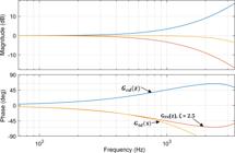
Bode plots of the notch filter, GFN(z), in brown; of the time delay, Gtd (s) = e−1.5Tss, in yellow; and of the proposed compensator, Gcd(z), in blue. It is observed that the phase lead of Gcd(z) compensates for the phase delay of Gtd(z).
The block diagram of the system incorporating the proposed compensator is shown in Fig. 12. Fig. 13, in turn, presents the root locus diagram for the compensated system, considering the four resonance frequencies listed in Table 1. This diagram illustrates the trajectories of the resonant poles as a function of the variation of the active damping loop gain. In comparison with the root locus diagram shown in Fig. 7, which refers to the uncompensated system, it can be observed that the poles associated with the frequencies fr2, fr3, and fr4 previously followed trajectories outside the unit circle, indicating instability. With the proposed compensator, however, these poles now follow trajectories that cross into the interior of the unit circle. This demonstrates that, with the compensator, poles that were previously unstable have become stable, even for frequencies above fs/6, which is the critical frequency for the uncompensated system.

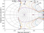
Root locus of the system with the proposed time delay compensator demonstrating the increase in the critical frequency, which consequently expands the stable region of the system.
A key feature in the diagram shown in Fig. 13 is the pole associated with the highest resonance frequency, fr4, represented in purple. Initially, this pole follows a trajectory inside the unit circle, but it becomes unstable when it crosses the frequency corresponding to 0.282fs, or approximately fs/3. Therefore, resonant poles with frequencies higher than fs/3 become unstable, indicating that this is the new critical frequency for the system with the proposed compensator. Based on this result, it can be concluded that the proposed compensator has increased the critical frequency fc from fs/6 to approximately fs/3, thus expanding the system’s stability region as intended.
V. EXPERIMENTAL RESULTS
This section presents the experimental results obtained to validate the theoretical analysis discussed earlier and to demonstrate the effectiveness of the proposed notch-filter-based compensator. The experimental setup, illustrated in Fig. 14, consists of a Typhoon HIL-402, which emulates the inverter and the grid as considered in the theoretical analysis, a dSPACE MicroLabBox DS1202, which implements the inverter control system, a Tektronix MSO46 mixed-signal oscilloscope, and a laptop. The tests were carried out under the conditions assumed in the theoretical analysis, using the parameters listed in Table 1.

A. Experimental Verification of Stability Regions
The initial experiments were conducted on the system with active damping (considering the condition Kad > Kp) but without the proposed compensator. Two LCL filters with different resonance frequencies were used: fr1 = 1.34kHz and fr2 = 1.67kHz, as listed in Table 1. The first resonance frequency, fr1, is lower than the uncompensated critical frequency fc, and is intended to demonstrate that the employed active damping effectively stabilizes the uncompensated system for resonance frequencies below fc. In contrast, when the resonance frequency is set to fr2 = fc the results clearly indicate the loss of stability, confirming that the uncompensated system becomes unstable once the critical frequency is reached. This behavior is presented in Fig. 15, which shows the experimental waveforms of the currents injected to the grid, i2abc, as the resonance frequency is switched from fr1 to fr2. The system remains stable at fr1 but becomes unstable at fr2, thus experimentally validating the critical frequency and the theoretical stability predictions for the uncompensated system.
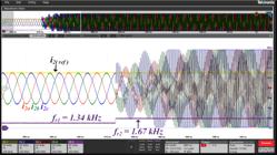
Experimental waveforms of the currents injected to the grid when the resonance frequency changes from fr1 < fc to fr2 = fc.
Continuing the experiments, the next step evaluates the uncompensated system behavior when the active damping loop gain satisfies Kad < Kp. Theoretically, this condition eliminates active damping, making the system behave as undamped. Thus, the system is stable for resonance frequencies above the critical frequency, fres > fc, and unstable below it, fres < fc. Fig. 16 experimentally confirms this prediction by showing the waveforms of currents injected to the grid with the active damping gain set to Kad < Kp. The system remains stable at fr3 > fc, but becomes unstable when the resonance frequency decreases to fr1 < fc. This clearly delineates the stability regions of the undamped system, in line with prior theoretical analysis.

Experimental waveforms of the currents injected to the grid when the resonance frequency changes from fr3 > fc to fr1 < fc with Kad < Kp, demonstrating the loss of active damping due to Kad.
B. Experimental Verification of Kad Constraints
As theoretically predicted in Section III and confirmed by the previous experimental results, the condition Kad > Kp is essential for maintaining the effectiveness of the active damping loop. In addition, the theoretical analysis establishes that Kad must remain within specific bounds to guarantee system stability, defining Kad(min) and Kad(max) as the lower and upper limits, respectively. To experimentally validate these limits, Fig. 17 illustrates the system response for Kad = Kad(min) and fres = fr1 under a step change in the current reference, where an overshoot of 16.1 % and a THD of 1.47 % are observed.

Experimental grid current waveform for Kad = Kad(min) and fres = fr1, under a step change in current reference. Overshoot: 16.1 %, THD: 1.47 %.
On the other hand, Fig. 18 shows the same waveform, with the only change being the active damping gain set to Kad = 0.045 — the midpoint between Kad(min) and Kad(max). A degradation in waveform quality is observed compared to the previous case, now exhibiting a THD of 2.5 % and an overshoot of 31.9 %.
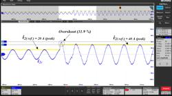
Experimental grid current waveform for Kad = Kad(avg) = 0.045 and fres = fr1, under a step change in current reference. Overshoot: 31.9 %, THD: 2.5 %.
Finally, adopting the theoretical value Kad = Kad(max), the current waveform exhibits higher harmonic distortion and overshoot values compared to the previous cases, as shown in Fig. 19, which presents a THD of 3.75 % and an overshoot of 35.6 %. It is important to note that with the gain set to Kad(max), the system behavior becomes significantly more oscillatory, approaching instability.

Experimental grid current waveform for Kad = Kad(max) and fres = fr1, under a step change in current reference. Overshoot: 35.6 %, THD: 3.75 %.
Figs. 17 to 19 show that increasing the gain Kad progressively deteriorates the system’s dynamic performance, resulting in larger overshoot, higher harmonic distortion, and a tendency toward instability. This behavior is consistent with the theoretical prediction from Section III, which associates higher Kad values with a reduction in the system’s phase margin—an effect that, in practice, manifests precisely as the degraded transient behavior observed in these figures.
C. Experimental Validation of the Proposed Compensator
To assess the effectiveness of the proposed controller, the following results present the system behavior with its implementation, enabling a direct comparison with the previous uncompensated case. Accordingly, Fig. 20 depicts the experimental grid current waveform under the same operating conditions as in Fig. 17, but now with the proposed controller enabled. A marked improvement in the system’s dynamic performance is observed, with the overshoot reduced from 16.1 % to 10.5 % and the THD from 1.47 % to 1.09 %, compared to the uncompensated case in Fig. 17.

Experimental grid current waveform for Kad = Kad(min) and fres = fr1 under a step change in current reference, with the proposed compensator. Overshoot: 10.5 %; THD: 1.01 %.
The improvement in the dynamic response observed in the latter result is a direct consequence of the expanded stability region provided by the proposed compensator. This expansion can be verified in Figure 21, which shows that the system remains stable even when the resonant frequency shifts from fr1 to fr2 = fc. As shown in Figure 15, under the same conditions, the system without the proposed compensator became unstable for fr2 = fc. Figure 22, in turn, demonstrates that the system remains stable even when the resonance frequency surpasses the critical frequency. In this case, the resonance frequency increases from fr1 to fr4, which is approximately 45 % higher than fc. Nevertheless, the system maintains stability, indicating that the critical frequency of the compensated system is higher than fr4.

Experimental grid current waveform with the proposed compensator when the resonance frequency shifts from fr1 < fc to fr2 = fc, demonstrating stable operation at both frequencies.

Experimental grid current waveform with the proposed compensator when the resonance frequency shifts from fr1 < fc to fr4 = fc, demonstrating stable operation at both frequencies.
Finally, when the resonance frequency is increased to fres = 2.8 kHz (fr4 + 0.4 kHz), the system becomes unstable, as illustrated in Fig. 23. This result confirms that the proposed compensator effectively extends the system’s critical frequency. With the compensator in place, the new critical frequency is established at 2.8 kHz, ensuring stable operation for all resonance frequencies below this threshold.

Experimental grid current waveform with the proposed compensator as the resonance frequency increases from fr4 to fr4 +0.4 kHz, illustrating the stability boundary.
VI. CONCLUSION
This paper presented a comprehensive strategy to enhance the stability of LCL-filtered grid-connected inverters. A detailed analysis of the active damping gain (Kad) revealed its critical impact on the system’s phase margin, establishing clear design guidelines for its selection to prevent performance degradation—an aspect often overlooked in the literature. The core of this work is a novel notch-filter-based compensator that directly counteracts system delays, successfully shifting the critical frequency from fs/6 to approximately fs/3 and thus expanding the stable operating region without computational overhead. Theoretical analyses and experimental validations on a hardware-in-the-loop (HIL) confirmed the proposed methodology’s effectiveness, demonstrating superior transient response, reduced harmonic distortion and robust stability, making it a promising solution for robust grid-connected inverter applications.
ACKNOWLEDGMENTS
The author acknowledges the Brazilian National Council for Scientific and Technological Development (CNPq) for funding this paper through project no. 406722/2022-6
-
PLAGIARISM POLICY
This article was submitted to the similarity system provided by Crossref and powered by iThenticate – Similarity Check.
DATA AVAILABILITY
The data used in this research is available in the body of the document.
REFERENCES
-
1 R. Teodorescu, F. Blaabjerg, M. Liserre, A. Dell’Aquila, “A stable three-phase LCL-filter based active rectifier without damping”, in 38th IAS Annual Meeting on Conference Record of the Industry Applications Conference, 2003., vol. 3, pp. 1552–1557 vol.3, 2003, doi:10.1109/IAS.2003.1257762.
» https://doi.org/10.1109/IAS.2003.1257762 -
2 J. Dannehl, C. Wessels, F. W. Fuchs, “Limitations of Voltage-Oriented PI Current Control of Grid-Connected PWM Rectifiers With LCL Filters”, IEEE Transactions on Industrial Electronics, vol. 56, no. 2, pp. 380–388, 2009, doi:10.1109/TIE.2008.2008774.
» https://doi.org/10.1109/TIE.2008.2008774 -
3 S. G. Parker, B. P. McGrath, D. G. Holmes, “Regions of Active Damping Control for LCL Filters”, IEEE Transactions on Industry Applications, vol. 50, no. 1, pp. 424–432, 2014, doi:10.1109/TIA.2013.2266892.
» https://doi.org/10.1109/TIA.2013.2266892 -
4 J. Wu, X. Jia, Y. Cui, D. Xu, “Grid-Connected CurrentDelayed Cascade Feedback Control Strategy for LCL Inverters”, in 2024 IEEE 7th International Electrical and Energy Conference (CIEEC), pp. 315–320, 2024, doi:10.1109/CIEEC60922.2024.10583223.
» https://doi.org/10.1109/CIEEC60922.2024.10583223 -
5 R. R. Kar, R. Wandhare, “Enhanced Stability and Control of Voltage Source Converters With LCL Filter in Weak Grid”, IEEE Journal of Emerging and Selected Topics in Industrial Electronics, vol. 6, no. 1, pp. 271–283, 2025, doi:10.1109/JESTIE.2024.3427363.
» https://doi.org/10.1109/JESTIE.2024.3427363 -
6 Z. Xin, X. Wang, P. C. Loh, F. Blaabjerg, “Grid-Current-Feedback Control for LCL-Filtered Grid Converters With Enhanced Stability”, IEEE Transactions on Power Electronics, vol. 32, no. 4, pp. 3216–3228, 2017, doi:10.1109/TPEL.2016.2580543.
» https://doi.org/10.1109/TPEL.2016.2580543 -
7 S. Bibian, H. Jin, “Time delay compensation of digital control for DC switchmode power supplies using prediction techniques”, IEEE Transactions on Power Electronics, vol. 15, no. 5, pp. 835–842, 2000, doi:10.1109/63.867672.
» https://doi.org/10.1109/63.867672 -
8 R. Raj Kar, R. Wandhare, “Passivity Principle-Based Active Damper Design to Enhance Stability of a Voltage Source Converter for Weak Grid Scenario”, IEEE Journal of Emerging and Selected Topics in Power Electronics, vol. 12, no. 5, pp. 5076–5089, 2024, doi:10.1109/JESTPE.2024.3406566.
» https://doi.org/10.1109/JESTPE.2024.3406566 -
9 D. Pan, X. Ruan, C. Bao, W. Li, X. Wang, “CapacitorCurrent-Feedback Active Damping With Reduced Computation Delay for Improving Robustness of LCLType Grid-Connected Inverter”, IEEE Transactions on Power Electronics, vol. 29, no. 7, pp. 3414–3427, 2014, doi:10.1109/TPEL.2013.2279206.
» https://doi.org/10.1109/TPEL.2013.2279206 -
10 X. Li, X. Wu, Y. Geng, X. Yuan, C. Xia, X. Zhang, “Wide Damping Region for LCL-Type Grid-Connected Inverter With an Improved Capacitor-Current-Feedback Method”, IEEE Transactions on Power Electronics, vol. 30, no. 9, pp. 5247– 5259, 2015, doi:10.1109/TPEL.2014.2364897.
» https://doi.org/10.1109/TPEL.2014.2364897 -
11 R. Peña-Alzola, M. Liserre, F. Blaabjerg, M. Ordonez, T. Kerekes, “A Self-commissioning Notch Filter for Active Damping in a Three-Phase LCL -Filter-Based Grid-Tie Converter”, IEEE Transactions on Power Electronics, vol. 29, no. 12, pp. 6754–6761, 2014, doi:10.1109/TPEL.2014.2304468.
» https://doi.org/10.1109/TPEL.2014.2304468 -
12 J. Ma, X. Wang, F. Blaabjerg, L. Harnefors, W. Song, “Accuracy Analysis of the Zero-Order Hold Model for Digital Pulse Width Modulation”, IEEE Transactions on Power Electronics, vol. 33, no. 12, pp. 10826–10834, 2018, doi:10.1109/TPEL.2018.2799819.
» https://doi.org/10.1109/TPEL.2018.2799819 - 13 B. Lathi, Linear Systems and Signals, 2nd edition, Oxford University Press, 2004.
-
14 A. G. Yepes, F. D. Freijedo, J. Doval-Gandoy, López, J. Malvar, P. Fernandez-Comesaña, “Effects of Discretization Methods on the Performance of Resonant Controllers”, IEEE Transactions on Power Electronics, vol. 25, no. 7, pp. 1692– 1712, 2010, doi:10.1109/TPEL.2010.2041256.
» https://doi.org/10.1109/TPEL.2010.2041256 -
15 D. Zmood, D. Holmes, “Stationary frame current regulation of PWM inverters with zero steady-state error”, IEEE Transactions on Power Electronics, vol. 18, no. 3, pp. 814–822, 2003, doi:10.1109/TPEL.2003.810852.
» https://doi.org/10.1109/TPEL.2003.810852 -
16 M. Liserre, F. Blaabjerg, S. Hansen, “Design and control of an LCL-filter-based three-phase active rectifier”, IEEE Transactions on Industry Applications, vol. 41, no. 5, pp. 1281–1291, 2005, doi:10.1109/TIA.2005.853373.
» https://doi.org/10.1109/TIA.2005.853373 -
17 M. B. Saïd-Romdhane, M. Naouar, I. S. Belkhodja, E. Monmasson, “Simple and systematic LCL filter design for threephase grid-connected power converters”, Mathematics and Computers in Simulation, vol. 130, pp. 181–193, 2016, doi:10.1016/j.matcom.2015.09.011.
» https://doi.org/10.1016/j.matcom.2015.09.011 -
18 M. Liserre, A. Dell’Aquila, F. Blaabjerg, “Genetic algorithm-based design of the active damping for an LCL-filter three-phase active rectifier”, IEEE Transactions on Power Electronics, vol. 19, no. 1, pp. 76–86, 2004, doi:10.1109/TPEL.2003.820540.
» https://doi.org/10.1109/TPEL.2003.820540 -
19 C. Liu, X. Zhang, L. Tan, F. Liu, “A novel control strategy of LCL-VSC based on notch concept”, in The 2nd International Symposium on Power Electronics for Distributed Generation Systems, pp. 343–346, 2010, doi:10.1109/PEDG.2010.5545767.
» https://doi.org/10.1109/PEDG.2010.5545767 -
20 Q. Zhao, F. Liang, W. Li, “A new control scheme for LCLtype grid-connected inverter with a Notch filter”, in The 27th Chinese Control and Decision Conference (2015 CCDC), pp. 4073–4077, 2015, doi:10.1109/CCDC.2015.7162637.
» https://doi.org/10.1109/CCDC.2015.7162637 -
21 L. Zhou, M. Preindl, “Optimal Tracking and Resonance Damping Design of Cascaded Modular Model Predictive Control for a Common-Mode Stabilized Grid-Tied LCL Inverter”, IEEE Transactions on Power Electronics, vol. 37, no. 8, pp. 9226–9240, 2022, doi:10.1109/TPEL.2022.3159599.
» https://doi.org/10.1109/TPEL.2022.3159599 -
22 Y. Jing, A. A. Durra, E. F. El-Saadany, “An Adaptive Digital Notch Filter Based on Grid Impedance Estimation for Improving LCL Filter Peformance”, in 2018 IEEE/PES Transmission and Distribution Conference and Exposition (TD), pp. 1–5, 2018, doi:10.1109/TDC.2018.8440296.
» https://doi.org/10.1109/TDC.2018.8440296 -
23 Z. Xin, X. Wang, P. C. Loh, F. Blaabjerg, “Realization of Digital Differentiator Using Generalized Integrator For Power Converters”, IEEE Transactions on Power Electronics, vol. 30, no. 12, pp. 6520–6523, 2015, doi:10.1109/TPEL.2015.2442414.
» https://doi.org/10.1109/TPEL.2015.2442414
Edited by
-
Associate Editor
Allan F. Cupertino https://orcid.org/0000-0001-8418-1985
-
Editor-in-Chief
Heverton A. Pereira https://orcid.org/0000-0003-0710-7815
History
-
Received
28 Aug 2025 -
Reviewed
02 Dec 2025 -
Reviewed
16 Jan 2026 -
Accepted
29 Jan 2026 -
Published
09 Mar 2026


