
 Dynamic Modeling and Experimental Validation of a Non-Isolated Bidirectional DC-DC Converter for Control-Oriented Design
ABSTRACT
This paper presents the mathematical modeling and control design of a high-power-density bidirectional DC-DC converter topology based on the three-state switching cell (3SSC). The operation stages corresponding to distinct duty cycle intervals are thoroughly analyzed, and state-space techniques are employed to derive small-signal dynamic models for both Buck and Boost modes. These models serve as the foundation for the design of digital compensators using classical frequency-domain control methods, ensuring compliance with predefined performance specifications. To verify the accuracy and applicability of the derived models, a comparative analysis is conducted between simulated and experimental closed-loop responses. The same compensators, designed using the mathematical models, are implemented both in circuit-level simulations and in a 2 kW hardware prototype operating at 200 V in Buck mode and 550 V in Boost mode, with a switching frequency of 20 kHz. The observed agreement in dynamic behavior under both reference and load disturbances validates the proposed models and confirms their suitability for control-oriented applications. This comparative validation approach represents the main contribution of the work, demonstrating that the small-signal plant models faithfully reproduce the real converter dynamics and can be reliably used in the design of digital controllers for bidirectional power conversion systems.
KEYWORDS
Bidirectional DC-DC converter; small-signal modeling; state-space averaging; experimental validation; cascaded control; electric vehicle
I. INTRODUCTION
In response to the global energy crisis, renewable energy sources have emerged as viable alternatives to mitigate reliance on fossil fuels [1]. Despite the continued dominance of fossil fuels in many regions, due to well-established infrastructure and a robust global market for exploration, refining, distribution, and storage, renewable energy options are steadily gaining prominence [2]–[4].
Vehicle electrification offers a significant opportunity to reduce atmospheric pollutant emissions [5], [6]. However, the driving force behind the advancement of this technology is the increasing stringency of regulations standardizing and limiting such emissions. In most countries, regulatory frameworks have progressively tightened, compelling automakers to design and certify vehicles that meet stricter emissions standards [7], [8].
The global market for electrically powered vehicles is experiencing rapid expansion, driven by efforts to phase out internal combustion engines [9]. Consequently, the traditional automotive industry must reinvent itself and face competition from a new generation of fully electric vehicles [10], [11]. Supporting this transformation, various sectors have developed to address diverse requirements, encompassing not only manufacturing but also the maintenance and servicing of these vehicles [12].
In energy systems, power transfer from a source to a load typically involves converting higher source voltage levels to match the load requirements [13], [14]. This is straightforward when the load exhibits passive behavior, allowing unidirectional power flow. However, modern applications, such as electric vehicles (EVs), hybrid electric vehicles (HEVs), and uninterruptible power supplies (UPS), demand bidirectional energy transfer capabilities [15]–[18]. These applications require power converters capable of supporting bidirectional energy flow, particularly in EV applications [19], [20]. Recent advancements in power electronics have led to the widespread adoption of bidirectional converters in transportation, driven by improvements in efficiency and power density [21]–[23].
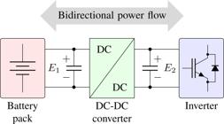
Bidirectional DC-DC power interface for energy transfer between the battery and DC link in EV applications.
The power converter analyzed in this paper, supports bidirectional energy flow in both Boost and Buck modes as shown in Figure 1. When power flows from the low-voltage (LV) side (E1) to the high-voltage (HV) side (E2), the circuit operates in Boost mode. Conversely, in Buck mode, power flows from the HV side (E2) to the LV side (E1). The power topology of the converter was originally proposed in [24] as shown in Figure 2.
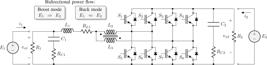
Non-isolated three-state switching cell (3SSC) based bidirectional DC-DC converter for mathematical modelling and transfer function validation proposed by [24].
Although both ports are connected to voltage sources, in one side the battery and another side the DC-link capacitor, in typical EV applications, as depicted in Figure 1, the small-signal modeling treats one side as an ideal voltage source and the opposite side as a resistive load. This standard approach simplifies the derivation of control-oriented transfer functions while accurately representing the dominant dynamics for controller design, as the resistive load effectively emulates the average power consumed by the downstream stage under nominal conditions.
In the context of EVs, precise mathematical models of converter operating modes are essential for designing effective controllers. EV applications demand well-regulated currents and voltages to ensure safe and reliable operation [25]. Lithium-ion batteries, commonly used in EVs, are sensitive devices with low tolerance for overcharging, overvoltage, and overdischarge, conditions that can lead to thermal runaway, a critical state characterized by excessive heat generation and potential fire hazards [26]. Thus, an accurate mathematical model is crucial for the bidirectional converter under study, as it handles both charging and discharging cycles for such batteries.
State-space modeling is the most appropriate approach for these complex systems, as it maintains mathematical simplicity even as the number of state variables increases. In contrast, traditional transfer-function-based methods often complicate the analysis of higher-order converters [27]. Moreover, state-space modeling accommodates both linear and nonlinear systems, offering efficient solutions for higher-order systems and overcoming the limitations of classical methods.
The growing demand for efficient and compact power conversion systems in electric vehicles (EVs) has driven research towards multi-functional converters capable of operating in both Buck and Boost modes. These converters must ensure high performance across a wide input voltage range while maintaining compactness and simplicity.
A promising topology addressing these requirements was recently proposed in [24], introducing a non-isolated DC-DC converter with reduced component count and extended voltage gain range with bidirectional power flow capability. While the original proposal focused on the converter’s static behavior and basic operation, [28] presents a theoretical analysis of the operating stages, along with the mathematical modeling and validation of the models for the converter operating in Buck mode. However, a detailed dynamic analysis, including smallsignal modeling and closed-loop control design, remains lacking in the literature.
This paper presents a comprehensive study of the converter introduced in [24], focusing on its small-signal modeling, controller design, and experimental validation. The main goal is to evaluate the dynamic behavior of the converter using the state-space averaging (SSA) technique and to verify the accuracy of the model through both simulation and experimental results. Additionally, a practical current and voltage-mode control system is implemented and tested, confirming the effectiveness of the modeling approach.
The contributions of this work can be summarized as follows:
-
Derivation of a small-signal model for the converter using SSA, covering buck and boost operating modes.
-
Design and implementation of a closed-loop current and voltage control system based on the developed model.
-
Experimental validation of the theoretical model through direct comparison with the converter’s dynamic behavior.
The paper is organized as follows. Section II presents the dynamic modeling of the converter operating in Boost mode, followed by Section III, which details the modeling for Buck mode. Section IV provides a comparative analysis between simulation and experimental results, highlighting the validation of the proposed small-signal models and control strategy. Finally, Section V summarizes the main contributions and conclusions of the work.
II. DYNAMIC MODELING IN BOOST MODE
The Boost and Buck modes are analyzed separately in the bidirectional DC-DC converter, resulting in distinct transfer functions for each operating mode, as presented in this paper. All derivations are carried out assuming Continuous Conduction Mode (CCM) for both modes. A state-space model is employed to derive equivalent mathematical representations of the converter’s operation in both modes [29].
Initially, the state-space variables relevant to each operational stage of the converter in Boost mode are defined. In this mode, the series resistances (ESR) of the main inductor L1 and the output capacitor C2 are explicitly included due to their noticeable influence on damping and losses. For simplicity, the ESRs of the auxiliary inductors L2 and L3 are neglected, as their values are significantly lower than that of L1 and their contribution to the overall system dynamics is minor in this topology.
The state-space variables utilized in this paper include the currents through inductors L1, L2, and L3, along with the voltage across the capacitor C2, as shown in (1) and (2), respectively.
Considering ideal switches in the mathematical models results in equivalent circuits that allow for the grouping of operation stages. By analyzing the eight operation stages of the Boost mode [30], it is possible to obtain similar stages by considering ideal diodes and suppressing non-conducting elements. Operation stages 1, 3, 5, and 7 can be represented by an equivalent circuit, as shown in Figure 3 (a). In this equivalent circuit, the inductors L2 and L3 are connected in anti-parallel, where the voltage across them is zero. The capacitor voltage C2 and its series resistance (Rse) RC2 represent the output voltage. The voltage and current levels in these operation stages are expressed in the state-space model in (4). Operation stages 2 and 6 share similarities in their equivalent circuits, as shown in Figure 3 (b). The voltage and current levels in these stages are represented in the state-space model by (5). Finally, operation stages 4 and 8 share the same equivalent circuit, as shown in Figure 3 (c), and are expressed by the state-space models in (6).

The vector-matrix representation of the system of equations is given by (3):
where,
The average AC model for the three operating equivalent circuits is derived from the state-space matrices in (4), (5), and (6) for the operation stages shown in Figure 3 (a), (b) and (c), respectively. The eight equivalent operation stages are represented by the state-space equation in (7).
The matrix K is the diagonal matrix containing the energy storage elements corresponding to each state variable. The explicit form of the state-space matrices for the equivalent circuits in Boost mode is presented in (1) and (2). In this operating mode, K is given by:
This formulation allows the state-space equations to be written in the standard form Kx˙ = Ax + Bu, where the left-hand side directly represents the physical relationships .
The nonlinear average state-space equations for the AC model are derived by rearranging the equations of each operation stage over a switching period Ts, based on the respective duty cycles d and d′. In Boost mode, the duty cycle d is within the range of 1/4 ≤ D < 1/2 of Ts.
where,
The dynamic behavior of power converters is commonly studied using small-signal linearization techniques. This approach consists of approximating the nonlinear averaged model around a steady-state operating point by introducing small AC perturbations in the state variables, input voltage, duty cycle, and output variables, as follows:
where uppercase letters denote DC steady-state values and hatted variables represent small-signal AC perturbations.
To obtain the small-signal model, the small AC perturbations in the state variables, duty cycle, and input voltage are substituted into the nonlinear averaged equations (9) and (10). This yields the following perturbed state-space representation for Boost mode in (17) and (18):
The nonlinearity of the averaged equations arises from the multiplication of time-varying quantities. Linearization around the steady-state operating point is mathematically possible for any perturbation amplitude; however, the resulting approximation is valid only when the AC perturbations are sufficiently small compared to the DC quiescent values. To obtain the small-signal model, small AC perturbations are introduced in the state variables, duty cycle portions, and input voltage. Upon expansion and collection of terms, DC terms, first-order AC terms, and second-order AC terms are obtained. The DC terms are removed to isolate the dynamic behavior, while the second-order AC terms are neglected due to their negligible magnitude under the small-signal assumption. This leaves only the first-order AC terms, yielding a linear time-invariant (LTI) smallsignal model suitable for frequency-domain analysis and controller design [31].
The Laplace transforms of the small-signal linearized equations yield the transfer functions that describe the variations in output voltage and inductor input current with respect to the duty cycle, as shown in (21) and (22), respectively. In both cases, input voltage variations are assumed to be zero.
where,
With (21) and (22), is obtained (26).
where,
To validate the obtained models, the converter circuit is simulated in open-loop configuration in Boost mode first, with parameters listed in Table 1. These parameter values were directly obtained from the converter design presented by [24].
In this simulation, a sinusoidal perturbation with amplitude of 1% of the nominal duty cycle is superimposed onto the steady-state duty cycle to excite the system while ensuring operation within the small-signal regime, with frequencies ranging from 10Hz to 100kHz. The frequency response of the disturbance both in terms of magnitude and phase is obtained by comparing the output variable of the simulated circuit with the response from the smallsignal model. The comparison of the frequency-domain responses, including the capacitor output voltage and the variations in the main inductor current as a function of the duty cycle, for both the simulated and calculated plants (22) and (21), is presented in Figure 4 for Boost mode.
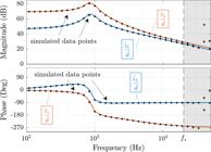
Bode diagrams for Boost mode comparing the small-signal mathematical model and circuit simulation results for ˆiL1(s)/dˆ(s) and vˆo(s)/dˆ(s), demonstrating strong agreement between both approaches.
The small-signal models are linearized around the nominal steady-state operating point corresponding to full load, with duty cycles D = 0.318 in Boost mode. Although the transfer functions exhibit mild dependence on the operating point, variations in load or reference produce only small changes in pole and zero locations. Moreover, any steady-state error arising from such variations is effectively eliminated by the integral action of the cascaded controllers, ensuring zero steady-state error in voltage regulation.
III. DYNAMIC MODELING IN BUCK MODE
For modeling the converter in buck operation mode, the main inductor L1 and coupled inductors L2 and L3 are retained as state variables, while the output filter capacitor is substituted as shown in (29).
By analyzing the circuits of the eight operation stages that constitute the buck operation mode, and assuming the same ideal conditions as in the previous section, it is observed that operation stages 2, 4, 6, and 8 are identical. Additionally, operation stages 1 and 5, as well as stages 3 and 7, are considered equivalent. Consequently, the circuits representing the eight operation stages in the buck operation mode can be reduced to three equivalent circuits, similar to the boost operation mode. In this operational mode, the intrinsic resistances Rse of the main inductor L1 and the output capacitor C1 are also considered in the model derivation. The ESRs of L2 and L3 are neglected for simplicity.
Figure 5 (a) presents operation stages 1 and 5, which were used to derive the models represented in (30). Operation stages 2, 4, 6, and 8 can be represented by an equivalent circuit, as shown in Figure 5 (b). In this equivalent circuit, the inductors L2 and L3 are connected in anti-parallel, resulting in zero voltage across them. The voltage across capacitor C1 and its series equivalent resistor RC1 represent the output voltage. The voltage and current levels in these operation stages are expressed in the state-space model in (31). Finally, operation stages 3 and 7 share the same equivalent circuit, as depicted in Figure 5 (c), and are represented by the state-space models in (30).

where,
The average AC model for the three operating equivalent circuits is derived from the state-space matrices: (30) for the operation stages shown in Figure 5 (a), (31) for the operation stages shown in Figure 5 (b), and (32) for the operation stages shown in Figure 5 (c).
The eight equivalent operation stages are described by the state-space equations in (7), as detailed in the previous section.
Now, the nonlinear average state-space equations for the AC model are obtained by rearranging the respective equations of each operation stage over a switching period Ts, based on the corresponding duty cycles d and d′. In this operational mode, the duty cycle D lies within the range of 0 < D < 1/4 of Ts.
where,
As in the Boost mode analysis, the matrix K is the diagonal matrix containing the energy storage elements corresponding to each state variable. In Buck mode, the only difference arises from the use of the low-voltage-side output capacitor C1; thus, K is given by:
The linearization process in Buck mode follows the same steps described in Section II. After substituting the perturbations into (34) and (35), expanding, and collecting terms, the DC and second-order AC terms are eliminated, retaining only the first-order AC contributions to form the small-signal LTI model.
Equations (38) and (39) are obtained by applying the Laplace transforms to the small-signal linearized equations. These transformations lead to the transfer functions that describe the variations in output voltage and the variations in the inductor input current as a function of the duty cycle. In both cases, input voltage variations are assumed to be zero.
where,
With (38) and (39) is obtained (41).
To validate the obtained models in Buck mode, the converter circuit is simulated in open-loop configuration. The steady-state operating point and linearization for Buck mode follow the same approach described in Section II, using the nominal values in Table 2.
The same disturbance amplitude and frequency variation from Boost mode were applied in Buck mode simulation. Both simulated and calculated plants (38) and (39), are presented in Figure 6 for Buck mode.

Bode diagrams for Buck mode comparing the small-signal mathematical model and circuit simulation results for
By analyzing the curves of the calculated models shown in Figure 4 and Figure 6, it can be observed that they closely match the curves obtained from circuit simulations. This agreement validates the small-signal models up to approximately half of the switching frequency (fs).
Therefore, the calculated models are appropriate for frequency-domain analysis and can effectively support the design of the converter’s controllers. As expected, the simulated circuit response exhibits disturbances near the switching frequency fs due to inherent switching effects.
It is worth mentioning that the current-to-voltage transfer function is directly derived from the previously validated small-signal transfer functions. Therefore, an individual verification of this function is not required. This transfer function is later employed in the design of a cascaded control structure, contributing to the experimental verification of the mathematically derived models.
IV. EXPERIMENTAL VERIFICATION
To ensure precise voltage regulation and effective dynamic response under varying load conditions, a cascaded control strategy is adopted. This approach consists of an inner current control loop and an outer voltage control loop. The inner loop regulates the inductor current, providing fast disturbance rejection and enhancing the overall system stability. The outer loop ensures that the output voltage accurately tracks the reference signal with minimal steady-state error. The small-signal transfer functions previously derived are employed in the design of both loops. The digital controllers are implemented in a digital signal controller (DSC) with sampling frequency equal to the switching frequency of 20 kHz. The proportional integral, and derivative gains are tuned to meet the specified crossover frequencies and phase margins, with integral action included in all controllers to ensure zero steady-state error.
All simulations and experimental tests presented in this section were conducted under load conditions to guarantee Continuous Conduction Mode (CCM) operation, as assumed in the modeling derivations. The measured inductor currents confirm CCM operation, with no zero-crossing observed in the waveforms across the entire tested operating range.
In both simulation and experimental setups, the same parameters were applied without any retuning. Since the control structure remained identical and the observed dynamic responses, such as rise time, settling time, and overshoot matched closely in both cases, it can be inferred that the modeled plant accurately represents the actual converter dynamics. In this context, the transfer function of the plant is the only element linking the model to the real system. Therefore, the consistency of the closed-loop behavior serves as strong evidence of the validity of the small-signal model.

Block diagram of the cascaded control system implemented for regulating output voltage and inductor current. All signals and transfer functions represent small-signal variations around the steady-state operating point.
A cascaded control scheme, illustrated in Fig. 7, is employed to regulate both output voltage and inductor current in both Boost and Buck modes. The inner current loop ensures fast disturbance rejection and current limiting, while the outer voltage loop provides accurate reference tracking with zero steady-state error due to the integral action in the controllers. To guarantee proper decoupling and stability, the voltage loop bandwidth is designed to be at least one decade lower than the current loop bandwidth. Typical design targets include crossover frequencies around 2 kHz for the inner loop and 100 Hz for the outer loop, with phase margins greater than 45° to ensure robust performance under load and reference variations. The detailed controller tuning for each operating mode, based on the derived small-signal transfer functions, is presented in the following subsections.
A. Boost Mode
When the converter operates in Boost mode, it transfers energy from the battery to the DC bus, which is typically used to power a traction inverter in an electric vehicle (EV). The voltage on the DC bus must remain stable, as any significant voltage drop could negatively affect the inverter stage and, consequently, engine performance. To maintain voltage stability, a fast transient response in the inductor current is essential, ensuring that when the load increases, the system can provide the necessary power quickly.
A cascade control scheme is also employed to regulate the converter in Boost mode. The same parameters used in the simulation and validation sections are adopted for the control design. A PID controller is used for the inner current loop, with the controller’s crossover frequency (fc) set to 2 kHz and a phase margin of 50°. The gains are Kp = 1.41×10⁴, Ki = 3.33×10⁷, and Kd = 0.708, tuned in the frequency domain to meet these specifications while ensuring fast current regulation and sufficient damping. In the outer voltage loop, the zero-crossing frequency must be kept lower than the current loop’s crossover frequency by at least one decade to prevent the voltage loop from interfering with the fast dynamics of the current loop. Therefore, a PI controller is designed for the voltage loop, with the fc set to 100Hz and a phase margin of 89°, ensuring closed-loop stability. The gains are Kp = 1.29 × 10⁵ and Ki = 1.51 × 10⁸, tuned in the frequency domain to achieve the specified bandwidth and stability margins while providing accurate reference tracking with zero steady-state error.

Experimental results in Boost mode recorded in a single 200 ms/div oscilloscope screenshot.
To validate the closed-loop performance, consecutive step-up and step-down load tests were conducted, as shown in Fig. 8 (a) and (b). The first test corresponds to a 40% change in nominal load. A second test corresponds to applying a nearly 50% power step from 10A to 6.72A, varying the voltage reference from 550V to 450V and back.
To further clarify the methodology adopted for the validation of the small-signal models, a comparative diagram is presented in Fig. 9. In this Figure, both the experimental setup and the mathematical model are subjected to the same input reference variation. Arrows indicate the direction of signal flow, emphasizing the shared input and the resulting outputs from the experimental converter and the simulated model. This schematic representation highlights the verification process adopted in this work, where the equivalence of responses under identical control conditions serves as validation of the modeled plant dynamics.

Comparison of simulated and experimental dynamic responses in Boost mode operation. Both systems were subjected to the same input reference variation where arrows indicate the origin of each response, distinguishing between experimental measurements and simulation results.
Examining the simulation results in Fig. 9, it can be observed that the converter operates at the nominal voltage of 550 V until 0.24 s. When the reference is stepped down, the output voltage takes approximately 40 ms to respond and settle at 450 V, with the inductor current iL1 reaching 6.72 A. The corresponding experimental result presents a slightly faster settling time of around 30 ms. A minor discrepancy is observed in the settling times. This small difference is attributed to unmodeled effects in the hardware implementation, such as digital control delays, sampling, computation, and PWM update, sensor bandwidth limitations, and additional parasitic elements not fully captured in the small-signal model or circuit simulation. Despite this, the overall dynamic behavior which are overshoot, rise time, and disturbance rejection shows excellent agreement, confirming the effectiveness of the proposed models and controllers for practical applications. To further evaluate the performance of the control system under sudden load variations, an additional test was conducted. The converter was initially operated with a resistive load totaling 142 Ω, representing nominal current conditions. At a specific moment during operation, an additional 56 Ω resistor was inserted in series, resulting in a 40% reduction in load current. The resulting load step caused a voltage undershoot of 69V with 12.5% of the 550V reference in simulation and 46V around 8.3% of the reference in the experimental prototype. Both cases presented a recovery time of approximately 25ms. The smaller experimental undershoot is attributed to unmodeled dynamics and implementation effects, while the nearly identical recovery time confirms the accuracy of the dominant poles and the effectiveness of the cascaded controllers in disturbance rejection.
B. Buck Mode
When the converter operates in Buck mode, energy flows from the DC bus to the battery. This occurs because the traction system, which was initially powered by the battery, now functions as a generator, regenerating energy.
For the Buck mode control design, the same parameters used in the small-signal model validation simulation, as described in the previous section, are adopted. A PID controller is implemented for the current loop, achieving a phase margin of 53.8° with a fc of 2kHz, ensuring closed-loop stability. The gains are Kp = 1.1×10⁴, Ki = 2.59×10⁷, and Kd = 0.551, tuned in the frequency domain to provide fast current regulation and adequate damping. The voltage loop is stable with a crossover frequency of 40Hz, however, the phase margin is excessively high. To optimize the phase margin, a PI controller with an additional pole positioned at the switching frequency of 20kHz is designed for the voltage loop. The gains are Kp = 7.54 × 10⁴ and Ki = 7.72 × 10⁷, resulting in a crossover frequency fc of 100 Hz and a phase margin of 88°. This extra pole configuration ensures effective attenuation of switching ripple.
To validate the closed-loop performance in Buck mode, consecutive step-up and step-down load tests were also conducted, as shown in Fig. 10 (a) and (b). The first test corresponds to a 22% change in nominal load. A second test corresponds to varying the voltage reference from 200V to 150V and back.

Experimental results in Buck mode recorded in a single 200 ms/div oscilloscope screenshot.
To evaluate the controller’s performance under a reference voltage disturbance, a 50V step-up was applied. Figure 11 presents the simulated and experimental results for this voltage reference step-up scenario. The converter initially operates at the nominal reference voltage of 150V until 0.20s. Upon the step-up, the controller responds within approximately 60ms in simulation, settling the output voltage at the new reference of 200V, with the inductor current iL1 reaching 10A. In the experimental result, the system settles within 50ms. Additionally, a load change test was performed to assess the system’s response to sudden variations in load demand. Starting from nominal operation with a resistive load of 15Ω, an additional resistor was added, resulting in a 22% decrease in total load resistance. This sudden increase in load current triggered a corresponding control action and the converter successfully compensated for the load variation. The load removal produced a voltage overshoot of 23.6V (12.5%) in simulation and 12.5V (6.25%) in experiment, with recovery times of 33ms and around 40ms, respectively. The reduced experimental overshoot stems from parasitic damping and sensor filtering, while the close recovery times confirm the model’s accuracy in representing the dominant dynamics. This test not only demonstrated the effectiveness of the cascaded control strategy under significant load transients but also experimentally verified the accuracy of the previously developed mathematical model.

Simulated and experimental dynamic responses in Buck mode under the same reference step. Arrows indicate the signal origin, emphasizing the close match between the model prediction and the measured converter behavior.
V. CONCLUSION
This paper presented the dynamic modeling and validation of a bidirectional DC-DC converter, supported by both simulation and experimental results. Theoretical small-signal models were derived for the equivalent circuits operating in both Buck and Boost modes.
In conclusion, a detailed analysis of the operating stages combined with the state-space averaging technique yielded accurate dynamic models for the bidirectional converter in both Buck and Boost modes. The validation process confirmed the models’ ability to faithfully reproduce the converter’s behavior, as evidenced by the close agreement between the calculated transfer functions and the simulated frequency responses, with matching characteristics observed up to nearly half the switching frequency.
Although experimental frequency-domain measurements were not performed, the closed-loop step responses to load and reference disturbances effectively validate the models across a broad frequency spectrum. A step input inherently contains energy over all frequencies of interest, and the excellent match between simulated and experimental transient responses demonstrates that the small-signal models capture the dominant dynamics required for robust controller design. These results reinforce the suitability and practical applicability of the proposed models for control-oriented design in bidirectional power conversion systems.
A key contribution of this work lies in the direct comparison between simulation and experimental results under identical conditions. The same controllers, designed using the linearized models, were applied to both environments without retuning. The close match in transient responses serves as strong evidence of the model’s accuracy and practical relevance. Experimental tests in both Boost and Buck modes, using cascaded current control, confirmed that the controllers respond effectively to variations in voltage reference and load. The validation presented focuses primarily on load and reference disturbances, which are the most common and critical in EV battery charging/discharging applications. Although direct input-voltage disturbance tests were not performed, the close agreement between simulation and experimental closed-loop responses under load steps indirectly confirms the model’s ability to reject input variations. Although the control strategy is designed to support bidirectional operation, experimental tests of mode transitions were not performed in this study. Future work may include such validation to demonstrate the robustness of the controllers under continuous power flow reversal. The experimental converter performance remained consistent with simulations thus validating the theoretical models and their suitability for applications such as electric vehicles.
ACKNOWLEDGMENT
This work was supported in part by the Coordenação de Aperfeiçoamento de Pessoal de Nível Superior – Brasil (CAPES) – Finance Code 001, in part by the Conselho Nacional de Desenvolvimento Científico e Tecnológico (CNPq) under Process numbers, 303278/2023-4, and 405061/2023-4, and by Fundação de Amparo à Pesquisa e Inovação do Estado de Santa Catarina (FAPESC), SC, Brazil. The authors are grateful to UDESC and FURB Universities.
PLAGIARISM POLICY
DATA AVAILABILITY
The data used in this research is available in the body of the document.
REFERENCES
-
1 Y. Li, Y. Wang, Y. Guan, D. Xu, “Design and Optimization of High-Gain Bidirectional DC–DC Converter for Electric Vehicles”, IEEE Trans Power Electron, vol. 38, no. 9, pp. 11221– 11232, 2023, doi:10.1109/TPEL.2023.3285627.
» https://doi.org/10.1109/TPEL.2023.3285627 -
2 A. Gupta, R. K. Singh, J. Paul, M. Sharma, S. Joshi, “BatteryOperated Electric Vehicles (BOEVs) Adoption in India: Analysis of Barriers and Strategies”, IEEE Trans Eng Manage, vol. 71, pp. 7076–7087, 2024, doi:10.1109/TEM.2023.3253621.
» https://doi.org/10.1109/TEM.2023.3253621 -
3 K. Strunz, E. Abbasi, D. N. Huu, “DC Microgrid for Wind and Solar Power Integration”, IEEE J Emerg Sel Top Power Electron, vol. 2, no. 1, pp. 115–126, 2014, doi:10.1109/JESTPE.2013.2294738.
» https://doi.org/10.1109/JESTPE.2013.2294738 -
4 J. Fang, H. Deng, N. Tashakor, F. Blaabjerg, S. M. Goetz, “State-Space Modeling and Control of Grid-Tied Power Converters With Capacitive/Battery Energy Storage and Grid-Supportive Services”, IEEE J Emerg Sel Top Power Electron, vol. 11, no. 1, pp. 234–250, 2023, doi:10.1109/JESTPE.2021.3101527.
» https://doi.org/10.1109/JESTPE.2021.3101527 -
5 Z. Hu, R. T. Mehrjardi, M. Ehsani, “On the Lifetime Emissions of Conventional, Hybrid, Plug-in Hybrid and Electric Vehicles”, IEEE Trans Ind Appl, vol. 60, no. 2, pp. 3502–3511, 2024, doi:10.1109/TIA.2023.3330950.
» https://doi.org/10.1109/TIA.2023.3330950 -
6 E. Dos Reis, R. Parizotto, L. R. Rocha, E. C. Goltz, R. P. Vieira, P. R. Eckert, “Dynamic Model and Drive of Multiphase Yasa Electric Machine for Electric Traction”, Eletrônica de Potência, vol. 28, no. 1, pp. 17–27, Jan. 2023, doi:10.18618/rep.2023.1.0030.
» https://doi.org/10.18618/rep.2023.1.0030 -
7 H. Wouters, W. Martinez, “Bidirectional Onboard Chargers for Electric Vehicles: State-of-the-Art and Future Trends”, IEEE Trans Power Electron, vol. 39, no. 1, pp. 693–716, 2024, doi:10.1109/TPEL.2023.3319996.
» https://doi.org/10.1109/TPEL.2023.3319996 -
8 E. Martinez-Vera, P. Banuelos-Sanchez, “Review of Bidirectional DC-DC Converters and Trends in Control Techniques for Applications in Electric Vehicles”, IEEE Lat Am Trans, vol. 22, no. 2, pp. 144–155, 2024, doi:10.1109/TLA.2024.10412031.
» https://doi.org/10.1109/TLA.2024.10412031 -
9 S. Mukherjee, J. M. Ruiz, P. Barbosa, “A High Power Density Wide Range DC–DC Converter for Universal Electric Vehicle Charging”, IEEE Trans Power Electron, vol. 38, no. 2, pp. 1998–2012, 2023, doi:10.1109/TPEL.2022.3217092.
» https://doi.org/10.1109/TPEL.2022.3217092 -
10 A. Upadhyaya, C. Mahanta, “An Overview of Battery Based Electric Vehicle Technologies With Emphasis on Energy Sources, Their Configuration Topologies and Management Strategies”, IEEE Trans Intell Transp Syst, vol. 25, no. 2, pp. 1087–1111, 2024, doi:10.1109/TITS.2023.3316191.
» https://doi.org/10.1109/TITS.2023.3316191 -
11 C. P. Ragasudha, S. Hemamalini, “Performance Analysis of a High Gain Bidirectional DC-DC Converter Fed Drive for an Electric Vehicle With Battery Charging Capability During Braking”, IEEE Access, vol. 12, pp. 14499–14511, 2024, doi:10.1109/ACCESS.2024.3357726.
» https://doi.org/10.1109/ACCESS.2024.3357726 -
12 F. Blaabjerg, H. Wang, I. Vernica, B. Liu, P. Davari, “Reliability of Power Electronic Systems for EV/HEV Applications”, Proc IEEE, vol. 109, no. 6, pp. 1060–1076, 2021, doi:10.1109/JPROC.2020.3031041.
» https://doi.org/10.1109/JPROC.2020.3031041 -
13 V. F. Pires, A. Cordeiro, C. Roncero-Clemente, S. Rivera, T. Dragičević, “DC–DC Converters for Bipolar Microgrid Voltage Balancing: A Comprehensive Review of Architectures and Topologies”, IEEE J Emerg Sel Top Power Electron, vol. 11, no. 1, pp. 981–998, 2023, doi:10.1109/JESTPE.2022.3208689.
» https://doi.org/10.1109/JESTPE.2022.3208689 -
14 T. Sojoudi, M. Sarhangzadeh, J. Olamaei, J. F. Ardashir, “An Extendable Bidirectional High-Gain DC–DC Converter for Electric Vehicle Applications Equipped With IOFL Controller”, IEEE Trans Power Electron, vol. 38, no. 8, pp. 9767–9779, 2023, doi:10.1109/TPEL.2023.3265765.
» https://doi.org/10.1109/TPEL.2023.3265765 -
15 S. Sarkar, A. Das, “An Isolated Single Input-Multiple Output DC–DC Modular Multilevel Converter for Fast Electric Vehicle Charging”, IEEE Journal of Emerging and Selected Topics in Industrial Electronics, vol. 4, no. 1, pp. 178–187, 2023, doi:10.1109/JESTIE.2022.3221006.
» https://doi.org/10.1109/JESTIE.2022.3221006 -
16 I. Kougioulis, A. Pal, P. Wheeler, M. R. Ahmed, “An Isolated Multiport DC–DC Converter for Integrated Electric Vehicle OnBoard Charger”, IEEE J Emerg Sel Top Power Electron, vol. 11, no. 4, pp. 4178–4198, 2023, doi:10.1109/JESTPE.2023.3276048.
» https://doi.org/10.1109/JESTPE.2023.3276048 -
17 J. Wan, F. Liu, Y. Li, K.-Z. Liu, “An Efficient Interleaved Bidirectional DC–DC Converter With Shared Soft-Switching Auxiliary Circuit”, IEEE Trans Power Electron, vol. 38, no. 11, pp. 14139–14149, 2023, doi:10.1109/TPEL.2023.3275641.
» https://doi.org/10.1109/TPEL.2023.3275641 -
18 M. Abdolahi, S. Hosseinnataj, M. Norouzian, J. Adabi, E. Pouresmaeil, “Bidirectional Dual-Input Single-Output DC-DC Converter Based on Passivity Control Strategy”, IEEE Open Journal of Power Electronics, vol. 5, pp. 1227–1242, 2024, doi:10.1109/OJPEL.2024.3444914.
» https://doi.org/10.1109/OJPEL.2024.3444914 -
19 W. C. Leal, M. O. Godinho, R. F. Bastos, C. R. de Aguiar, G. H. F. Fuzato, R. Q. Machado, “Cascaded Interleaved DC–DC Converter for a Bidirectional Electric Vehicle Charging Station”, IEEE Trans Ind Electron, vol. 71, no. 4, pp. 3708– 3717, 2024, doi:10.1109/TIE.2023.3273281.
» https://doi.org/10.1109/TIE.2023.3273281 -
20 F. Wang, Y. Wang, Z. Dong, S. Wang, “Multiphase Low Stresses High Step-Up DC–DC Converter With Self-Balancing Capacitor Voltages and Self-Averaging Inductor Currents”, IEEE Trans Power Electron, vol. 37, no. 6, pp. 6913–6926, 2022, doi:10.1109/TPEL.2021.3133613.
» https://doi.org/10.1109/TPEL.2021.3133613 -
21 F. G. Nimitti, A. M. S. S. Andrade, “Synthesis and Classification of Boost/Buck Structures for Getting Transformerless Hybrid Bidirectional DC–DC Converters”, IEEE Trans Power Electron, vol. 39, no. 8, pp. 10048–10056, 2024, doi:10.1109/TPEL.2024.3395362.
» https://doi.org/10.1109/TPEL.2024.3395362 -
22 S. Wang, H. Li, Z. Zhang, M. Li, J. Zhang, X. Ren, Q. Chen, “Multifunction Capability of SiC Bidirectional Portable Chargers for Electric Vehicles”, IEEE J Emerg Sel Top Power Electron, vol. 9, no. 5, pp. 6184–6195, 2021, doi:10.1109/JESTPE.2021.3052841.
» https://doi.org/10.1109/JESTPE.2021.3052841 -
23 S. Zeljkovic, T. Reiter, D. Gerling, “Efficiency Optimized SingleStage Reconfigurable DC/DC Converter for Hybrid and Electric Vehicles”, IEEE J Emerg Sel Top Power Electron, vol. 2, no. 3, pp. 496–506, 2014, doi:10.1109/JESTPE.2014.2305739.
» https://doi.org/10.1109/JESTPE.2014.2305739 -
24 R. Mayer, M. B. E. Kattel, S. V. G. Oliveira, “Multiphase Interleaved Bidirectional DC/DC Converter With Coupled Inductor for Electrified-Vehicle Applications”, IEEE Trans Power Electron, vol. 36, no. 3, pp. 2533–2547, 2021, doi:10.1109/TPEL.2020.3015390.
» https://doi.org/10.1109/TPEL.2020.3015390 -
25 F. G. Nimitti, A. M. Andrade, “Unraveling Bidirectional Converter Capabilities: a Didactic Platform for Proving DualDirection Operation Based on Current Injection”, Eletrônica de Potência, vol. 28, no. 4, pp. 287–294, Dec. 2023, doi:10.18618/rep.2023.4.0020.
» https://doi.org/10.18618/rep.2023.4.0020 -
26 N. Lyu, Y. Jin, R. Xiong, S. Miao, J. Gao, “Real-Time Overcharge Warning and Early Thermal Runaway Prediction of Li-Ion Battery by Online Impedance Measurement”, IEEE Trans Ind Electron, vol. 69, no. 2, pp. 1929–1936, 2022, doi:10.1109/TIE.2021.3062267.
» https://doi.org/10.1109/TIE.2021.3062267 - 27 K. Ogata, Modern Control Engineering, 5th ed., Prentice Hall, 2010.
- 28 M. Wenk, R. Mayer, F. J. Zimann, S. V. G. Oliveira, A. L. Batschauer, “Buck-Mode Operation of a Non-Isolated Bidirectional DC-DC Converter for Electric Vehicles Applications: Analysis and Validation”, in Proc. Brazilian Power Electronics Conf. (COBEP), Oct. 2025.
- 29 J. G. Kassakian, M. F. Schlecht, G. C. Verghese, Principles of Power Electronics, Addison-Wesley series in electrical engineering, Addison-Wesley, 1991.
-
30 R. Mayer, M. B. E. Kattel, M. D. Possamai, C. Bruning, S. V. G. Oliveira, “Analysis of a multi–phase interleaved bidirectional DC/DC power converter with coupled inductor”, in Proc. Brazilian Power Electronics Conf. (COBEP), pp. 1–6, Nov. 2017, doi:10.1109/COBEP.2017.8257228.
» https://doi.org/10.1109/COBEP.2017.8257228 - 31 R. Erickson, D. Maksimović, Fundamentals of Power Electronics, 3 ed., Springer, 2001.


